M62254FP データシートの表示(PDF) - MITSUBISHI ELECTRIC
部品番号
コンポーネント説明
メーカー
M62254FP Datasheet PDF : 11 Pages
| |||
Mitsubishi Semiconductor < DIGI•ANA Interface >
M62254FP
Standard Battery Charger Controller
Word description:
td : The time after VDD reaching Reset release voltage to "High" Reset output.
tRT(1) : The time TC pin voltage changes from 0V to VTH2(L), when VDD is given.
tWD : The time TC pin voltage changes from VTH2(L) to VTH2(H).
tRT(2) : The time TC pin voltage changes from VTH2(H) to VTH2(L).
1. Regarding the pin 25 (Ctd pin) capacity and the delay time (td)
The delay time (td) of Reset output can be found using following equation.
td = 2x10 5 x Ctd (S)
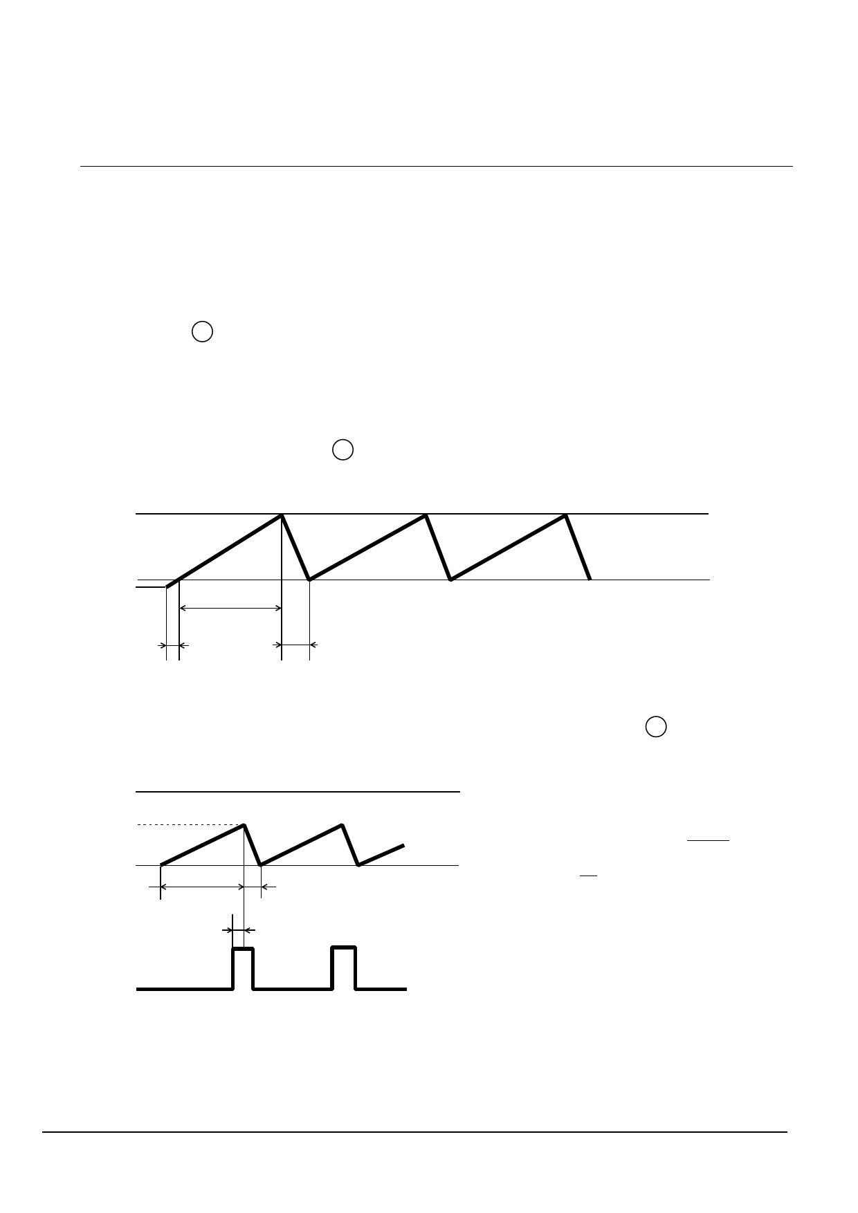
2. Regarding charge and discharge of pin 27 (TC pin)
When incorrect clock is given to the WD pin, the voltage level of TC pin will be changed as show below.
tWD
tRT(1)
tRT(2)
tRT(1) = 8 x 10 3 x Ctd (S)
tWD = 1 x 10 5 x CT (S)
tRT(2) = 2.5 x 10 4 x CT (S)
3. Regarding the input clock, input pulse width, charging time, and discharging time of pin 26 (WD pin)
When correct clock is given to the WD pin, the voltage level of TC pin will be changed as show below.
2.7V
xV
TC
WD
t1
t2
tWDIN(MIN)
0.2V
t1 = 1 x 10 5 x CT x x - 0.2
2.5
t2 = 1 x t1
4
Please, set the pulse width (tWDIN) more than tWDIN(MIN).
Share Link: 