MAX4665CSE データシートの表示(PDF) - Maxim Integrated
部品番号
コンポーネント説明
メーカー
MAX4665CSE Datasheet PDF : 12 Pages
| |||
5Ω, Quad, SPST,
CMOS Analog Switches
Pin Description
MAX4664
PIN
MAX4665
MAX4666
1, 16, 9, 8 1, 16, 9, 8 1, 16, 9, 8
2, 15,
10, 7
2, 15,
10, 7
2, 15,
10, 7
3,14, 11, 6
–
–
–
3,14, 11, 6
–
–
–
3, 6
–
–
14, 11
4
4
4
5
5
5
12
12
12
13
13
13
NAME
IN1, IN2,
IN3, IN4
COM1, COM2,
COM3, COM4
NC1, NC2,
NC3, NC4
NO1, NO2,
NO3, NO4
NO1, NO4
NC2, NC3
V-
GND
VL
V+
FUNCTION
Logic-Control Digital Inputs
Analog Switch, Common Terminals
Analog Switch, Normally Closed Terminals
Analog Switch, Normally Open Terminals
Analog Switch, Normally Open Terminal
Analog Switch, Normally Closed Terminal
Negative Analog Supply-Voltage Input. Connect to GND for single-
supply operation.
Ground
Logic-Supply Input
Positive Analog Supply Input
Applications Information
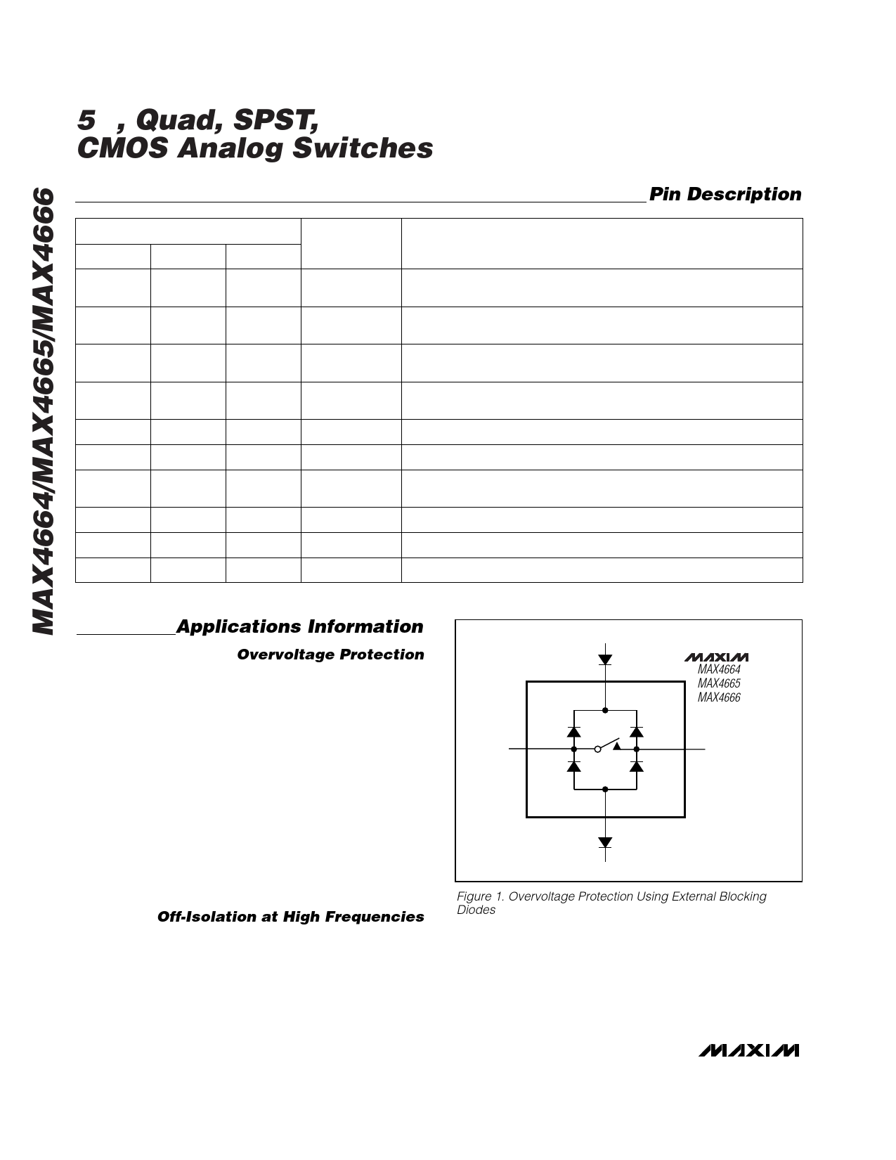
Overvoltage Protection
Proper power-supply sequencing is recommended for
all CMOS devices. Do not exceed the absolute maxi-
mum ratings, because stresses beyond the listed rat-
ings can cause permanent damage to the devices.
Always sequence V+ on first, then V-, followed by the
logic inputs, NO, or COM. If power-supply sequencing
is not possible, add two small signal diodes (D1, D2) in
series with supply pins (Figure 1). Adding diodes
reduces the analog signal range to one diode drop
below V+ and one diode drop above V-, but does not
affect the devices’ low switch resistance and low leak-
age characteristics. Device operation is unchanged,
and the difference between V+ and V- should not
exceed 44V. These protection diodes are not recom-
mended when using a single supply.
Off-Isolation at High Frequencies
In 50Ω systems, the high-frequency on-response of
these parts extends from DC to above 100MHz, with a
typical loss of -2dB. When the switch is turned off, how-
ever, it behaves like a capacitor, and off-isolation
decreases with increasing frequency. (Above 300MHz,
COM_
+15V
D1
V+
*
*
*
*
MAX4664
MAX4665
MAX4666
NO_
V-
D2
-15V * INTERNAL PROTECTION DIODES
Figure 1. Overvoltage Protection Using External Blocking
Diodes
the switch actually passes more signal turned off than
turned on.) This effect is more pronounced with higher
source and load impedances.
8 _______________________________________________________________________________________
Share Link: 