ICX054AL データシートの表示(PDF) - Sony Semiconductor
部品番号
コンポーネント説明
メーカー
ICX054AL Datasheet PDF : 17 Pages
| |||
ICX054AL
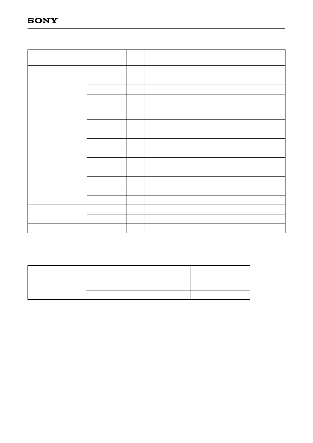
Clock Voltage Conditions
Item
Symbol
Min.
Typ.
Max.
Unit
Waveform
diagram
Remarks
Readout clock voltage VVT
14.55 15.0 15.45 V
1
VVH1, VVH2
–0.05 0 0.05 V
2
VVH = (VVH1+VVH2) /2
VVH3, VVH4
–0.2 0 0.05 V
2
VVL1, VVL2,
VVL3, VVL4
VφV
–9.0 –8.5 –8.0 V
7.8 8.5 9.05 V
2
VVL = (VVL3 + VVL4) /2
2
VφV = VVHn – VVLn (n = 1 to 4)
Vertical transfer clock
voltage
|VVH1 – VVH2|
VVH3 – VVH
–0.25
0.1 V
2
0.1 V
2
VVH4 – VVH
–0.25
0.1 V
2
VVHH
0.5 V
2 High-level coupling
VVHL
0.5 V
2 High-level coupling
VVLH
0.5 V
2 Low-level coupling
VVLL
0.5 V
2 Low-level coupling
Horizontal transfer
clock voltage
Reset gate clock
voltage
VφH
4.75 5.0 5.25 V
VHL
–0.05 0 0.05 V
VφRG
4.5 5.0 5.5 V
VRGLH – VRGLL
0.8 V
3
3
4
∗1
4 Low-level coupling
Substrate clock voltage VφSUB
22.5 23.5 24.5 V
5
∗1 The reset gate clock voltage need not be adjusted when reset gate clock is driven when the specifications
are as given below. In this case, the reset gate clock voltage setting indicated on the back of the image
sensor has not significance.
Item
Reset gate clock
voltage
Symbol Min.
VRGL
VφRG
–0.2
8.5
Typ.
0
9.0
Max.
Unit
Waveform
diagram
Remarks
0.2
V
4
9.5
V
4
–4–
Share Link: 