LT1237CG データシートの表示(PDF) - Linear Technology
部品番号
コンポーネント説明
メーカー
LT1237CG
Linear Technology

LT1237CG Datasheet PDF : 8 Pages
| |||
LT1237
APPLICATI S I FOR ATIO
Storage Capacitor Selection
The V+ and V – storage capacitors must be chosen care-
fully to insure low ripple and stable operation. The LT1237
charge pump operates in a power efficient Burst ModeTM
operation. When storage capacitor voltage drops below a
preset threshold, the oscillator is gated on until V+ and V–
are boosted up to levels exceeding a second threshold.
The oscillator then turns off, and current is supplied from
the V+ and V – storage capacitors.
The V – potential is monitored to control charge pump
operation. It is therefore important to insure lower V+
ripple than V – ripple, or erratic operation of the charge
pump will result. Proper operation is insured in most
applications by choosing the V+ filter capacitor to be at
least 5 times the V– filter capacitor value. If V+ is more
heavily loaded than V–, a larger ratio may be needed.
The V – filter capacitor should be selected to obtain low
ripple when the drivers are loaded, forcing the charge
pump into continuous mode. A minimum value 0.1µF is
suggested.
Do not attempt to reduce V– ripple when the charge pump
is in discontinuous Burst Mode operation. The ripple in
this mode is determined by internal comparator thresh-
olds. Larger storage capacitor values increase the burst
period, and do not reduce ripple amplitude.
Power Saving Operational Modes
The LT1237 has both shutdown and driver disable operat-
ing modes. These operating modes can optimize power
consumption based upon applications needs.
The On/Off shutdown control turns off all circuitry except
for Low-Q RX5. When RX5 detects a signal, this informa-
tion can be used to wake up the system for full operation.
If more than one line must be monitored, the driver disable
mode provides a power efficient operating option. The
driver disable mode turns off the charge pump and RS232
drivers, but keeps all five receivers active. Power con-
sumption in driver disable mode is 3mA from VCC.
Burst Mode is a trademark of Linear Technology Corporation
U
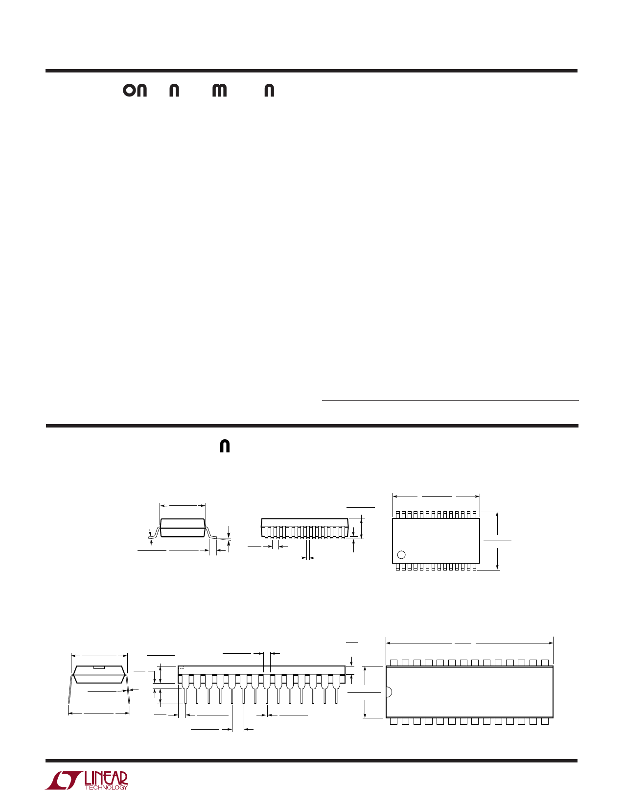
PACKAGE DESCRIPTIO Dimensions in inches (millimeters) unless otherwise noted.
0.205 – 0.212**
(5.20 – 5.38)
G Package
28-Lead Plastic SSOP (0.209)
(LTC DWG # 05-08-1640)
0° – 8°
0.068 – 0.078
(1.73 – 1.99)
0.397 – 0.407*
(10.07 – 10.33)
28 27 26 25 24 23 22 21 20 19 18 17 16 15
0.005 – 0.009 0.022 – 0.037
(0.13 – 0.22) (0.55 – 0.95)
0.0256
(0.65)
BSC 0.010 – 0.015
(0.25 – 0.38)
*DIMENSIONS DO NOT INCLUDE MOLD FLASH. MOLD FLASH
SHALL NOT EXCEED 0.006" (0.152mm) PER SIDE
**DIMENSIONS DO NOT INCLUDE INTERLEAD FLASH. INTERLEAD
FLASH SHALL NOT EXCEED 0.010" (0.254mm) PER SIDE
0.002 – 0.008
(0.05 – 0.21)
0.301 – 0.311
(7.65 – 7.90)
1 2 3 4 5 6 7 8 9 10 11 12 13 14 G28 SSOP 0694
NW Package
28-Lead PDIP (Wide 0.600)
(LTC DWG # 05-08-1520)
0.600 – 0.625
(15.240 – 15.875)
0.150 ± 0.005
(3.810 ± 0.127)
0.045 – 0.065
(1.143 – 1.651)
0.070
(1.778)
TYP
0.009 – 0.015
(0.229 – 0.381)
0.015
(0.381)
MIN
0.505 – 0.560*
(12.827 – 14.224)
+0.035
0.625 –0.015
( ) 15.87
+0.889
–0.381
0.125
(3.175)
MIN
0.035 – 0.080
(0.889 – 2.032)
0.100 ± 0.010
(2.540 ± 0.254)
0.018 ± 0.003
(0.457 ± 0.076)
*THESE DIMENSIONS DO NOT INCLUDE MOLD FLASH OR PROTRUSIONS.
MOLD FLASH OR PROTRUSIONS SHALL NOT EXCEED 0.010 INCH (0.254mm)
1.455*
(36.957)
MAX
28 27 26 25 24 23 22 21 20 19 18 17 16 15
1 2 3 4 5 6 7 8 9 10 11 12 13 14
N28 1197
Information furnished by Linear Technology Corporation is believed to be accurate and reliable.
However, no responsibility is assumed for its use. Linear Technology Corporation makes no represen-
tation that the interconnection of its circuits as described herein will not infringe on existing patent rights.
7
Share Link: