LZ2416J データシートの表示(PDF) - Sharp Electronics
部品番号
コンポーネント説明
メーカー
LZ2416J
Sharp Electronics

LZ2416J Datasheet PDF : 12 Pages
| |||
LZ2416J
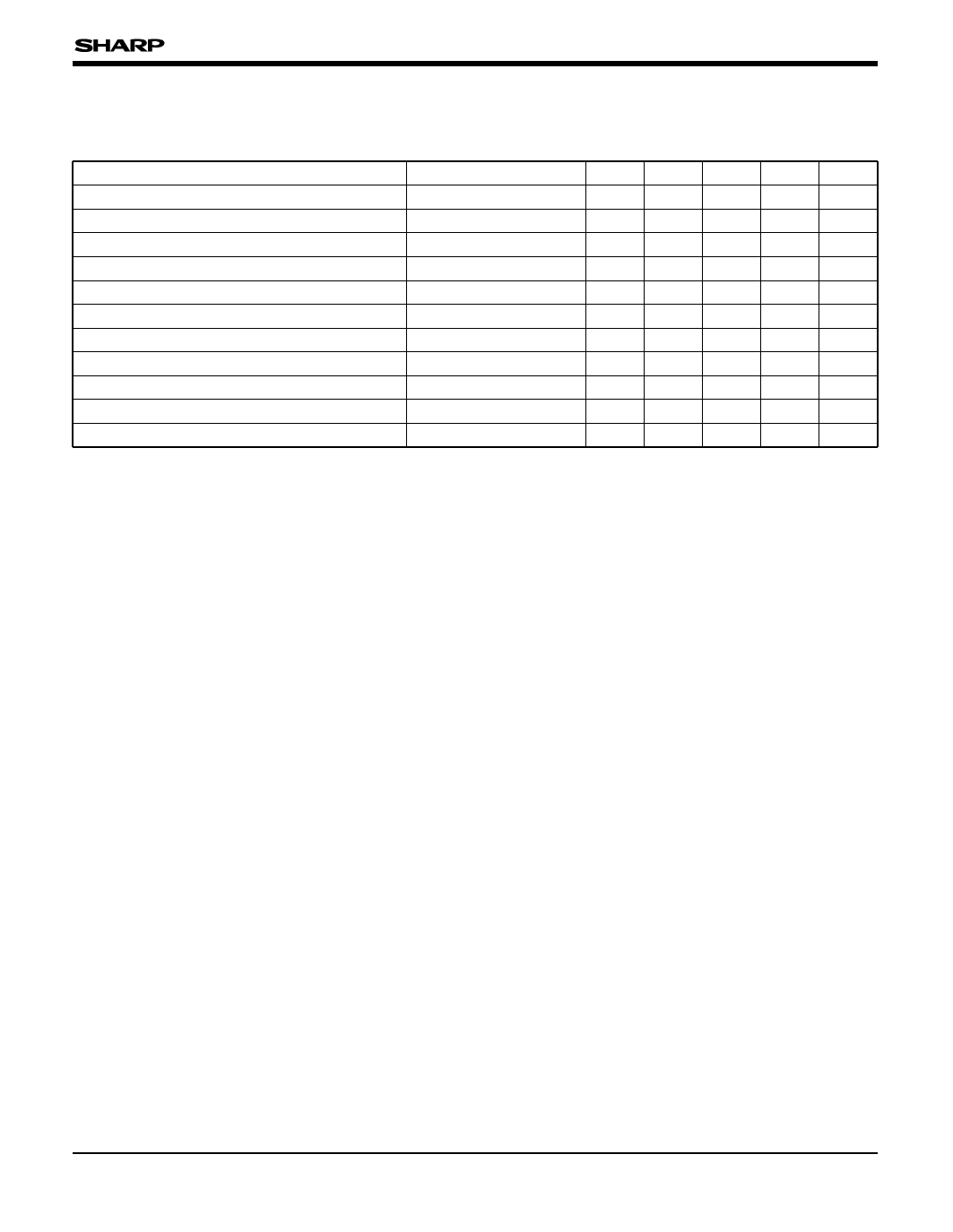
CHARACTERISTICS (Drive method : Field accumulation)
(TA = +25 ˚C, Operating conditions : The typical values specified in "RECOMMENDED OPERATING CONDITIONS".
Color temperature of light source : 3 200 K, IR cut-off filter (CM-500, 1 mmt) is used.)
PARAMETER
SYMBOL
MIN. TYP. MAX. UNIT NOTE
Standard output voltage
VO
150
mV
2
Photo response non-uniformity
PRNU
15
%
3
Saturation output voltage
VSAT
500
mV
4
Dark output voltage
VDARK
0.5
mV 1, 5
Dark signal non-uniformity
DSNU
0.5
mV 1, 6
Sensitivity
R
450
mV
7
Smear ratio
SMR
–84
dB
8
Image lag
AI
1.0 %
9
Blooming suppression ratio
ABL
1 000
10
Output transistor drain current
IOD
4.0 8.0 mA
Output impedance
RO
400
$
NOTES :
• VOFD should be adjusted to the minimum voltage such
that ABL satisfy the specification, or to the value
displayed on the device.
1. TA = +60 ˚C
2. The average output voltage under uniform illumination.
The standard exposure conditions are defined as when
Vo is 150 mV.
3. The image area is divided into 10 x 10 segments under
the standard exposure conditions. Each segment's
voltage is the average output voltage of all pixels within
the segment. PRNU is defined by (Vmax – Vmin)/Vo,
where Vmax and Vmin are the maximum and minimum
values of each segment's voltage respectively.
4. The image area is divided into 10 x 10 segments. Each
segment's voltage is the average output voltage of all
pixels within the segment. VSAT is the minimum
segment's voltage under 10 times exposure of the
standard exposure conditions.
5. The average output voltage under non-exposure
conditions.
6. The image area is divided into 10 x 10 segments under
non-exposure conditions. DSNU is defined by (Vdmax –
Vdmin), where Vdmax and Vdmin are the maximum and
minimum values of each segment's voltage respectively.
7. The average output voltage when a 1 000 lux light
source with a 90% reflector is imaged by a lens of F4,
f50 mm.
8. The sensor is exposed only in the central area of V/10
square with a lens at F4, where V is the vertical image
size. SMR is defined by the ratio of the output voltage
detected during the vertical blanking period to the
maximum output voltage in the V/10 square.
9. The sensor is exposed at the exposure level
corresponding to the standard conditions. AI is defined
by the ratio of the output voltage measured at the 1st
field during the non-exposure period to the standard
output voltage.
10. The sensor is exposed only in the central area of V/10
square, where V is the vertical image size. ABL is
defined by the ratio of the exposure at the standard
conditions to the exposure at a point where blooming is
observed.
4
Share Link: