MAX1213N データシートの表示(PDF) - Maxim Integrated
部品番号
コンポーネント説明
メーカー
MAX1213N Datasheet PDF : 21 Pages
| |||
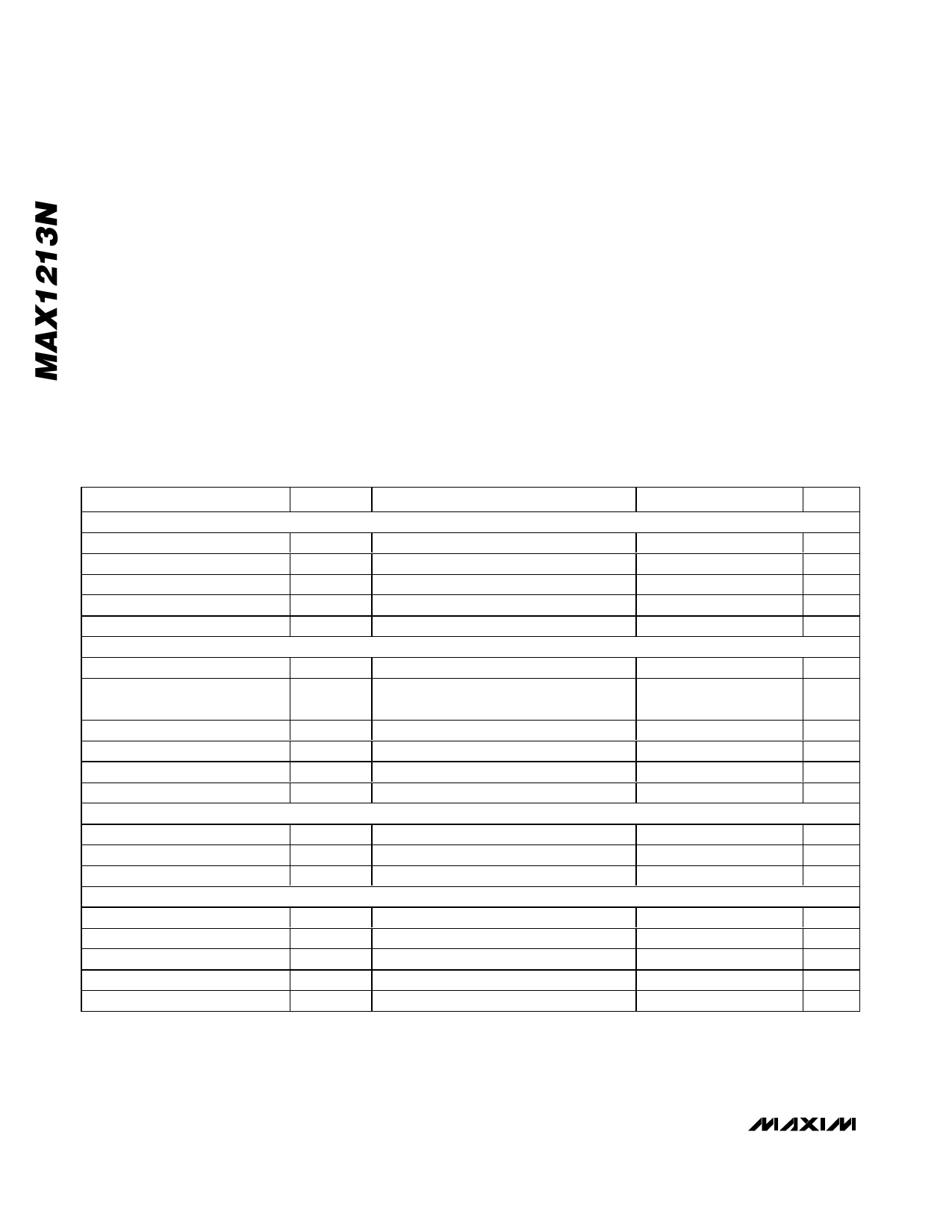
1.8V, Low-Power, 12-Bit, 170Msps
ADC for Broadband Applications
ABSOLUTE MAXIMUM RATINGS
AVCC to AGND ......................................................-0.3V to +2.1V
OVCC to OGND .....................................................-0.3V to +2.1V
AVCC to OVCC .......................................................-0.3V to +2.1V
AGND to OGND ....................................................-0.3V to +0.3V
INP, INN to AGND ....................................-0.3V to (AVCC + 0.3V)
All Digital Inputs to AGND........................-0.3V to (AVCC + 0.3V)
REFIO, REFADJ to AGND ........................-0.3V to (AVCC + 0.3V)
All Digital Outputs to OGND ....................-0.3V to (OVCC + 0.3V)
Continuous Power Dissipation (TA = +70°C, multilayer board)
68-Pin QFN-EP (derate 41.7mW/°C above +70°C).....3333mW
Current into Any Pin..........................................................±50mA
Operating Temperature Range ...........................-40°C to +85°C
Junction Temperature .....................................................+150°C
Storage Temperature Range ............................-60°C to +150°C
Lead Temperature (soldering,10s) ..................................+300°C
Stresses beyond those listed under “Absolute Maximum Ratings” may cause permanent damage to the device. These are stress ratings only, and functional
operation of the device at these or any other conditions beyond those indicated in the operational sections of the specifications is not implied. Exposure to
absolute maximum rating conditions for extended periods may affect device reliability.
ELECTRICAL CHARACTERISTICS
(AVCC = OVCC = 1.8V, AGND = OGND = 0, fSAMPLE = 170MHz, differential clock input drive, 0.1µF capacitor on REFIO, internal ref-
erence, digital output pins differential RL = 100Ω. Limits are for TA = -40°C to +85°C, unless otherwise noted. Typical values are at
TA = +25°C.) (Note 1)
PARAMETER
DC ACCURACY
Resolution
Integral Nonlinearity
Differential Nonlinearity
Transfer Curve Offset
Offset Temperature Drift
ANALOG INPUTS (INP, INN)
Full-Scale Input Voltage Range
Full-Scale Range Temperature
Drift
Common-Mode Input Voltage
Differential Input Capacitance
Differential Input Resistance
Full-Power Analog Bandwidth
REFERENCE (REFIO, REFADJ)
Reference Output Voltage
Reference Temperature Drift
REFADJ Input High Voltage
SAMPLING CHARACTERISTICS
Maximum Sampling Rate
Minimum Sampling Rate
Clock Duty Cycle
Aperture Delay
Aperture Jitter
SYMBOL
INL
DNL
VOS
VFS
VCM
CIN
RIN
FPBW
VREFIO
VREFADJ
fSAMPLE
fSAMPLE
tAD
tAJ
CONDITIONS
fIN = 10MHz (Note 2)
No missing codes (Note 2)
(Note 2)
Internally self-biased
REFADJ = AGND
Used to disable the internal reference
Set by clock-management circuit
Figures 5, 11
Figure 11
MIN TYP MAX UNITS
12
Bits
-2
±0.55
+2
LSB
-1.0 ±0.3 +1.3 LSB
-5
+5
mV
±10
µV/°C
1160
1380
±50
0.74
2.5
1.8
700
mVP-P
ppm/°C
V
pF
kΩ
MHz
1.18 1.24
90
AVCC - 0.3
1.30
V
ppm/°C
V
170
20
40 to 60
620
0.15
MHz
MHz
%
ps
psRMS
2 _______________________________________________________________________________________
Share Link: 