MAX1820 データシートの表示(PDF) - Maxim Integrated
部品番号
コンポーネント説明
メーカー
MAX1820 Datasheet PDF : 18 Pages
| |||
WCDMA Cellular Phone 600mA
Buck Regulators
ABSOLUTE MAXIMUM RATINGS
BATT, OUT (FB), SHDN, SYNC, SKIP,
REF to GND .......................................................-0.3V to +6.0V
PGND to GND .......................................................-0.3V to +0.3V
LX, COMP to GND...................................-0.3V to (VBATT + 0.3V)
Output Short-Circuit Duration ............................................Infinite
Continuous Power Dissipation (TA = +70°C)
3 ✕ 4 UCSP (derate 10.4mW/°C above +70°C)............832mW
10-Pin µMAX (derate 5.6mW/°C above +70°C) ...........444mW
Operating Temperature Range ...........................-40°C to +85°C
Junction Temperature ......................................................+150°C
Storage Temperature Ranges
3 ✕ 4 UCSP ....................................................-40°C to +150°C
10-Pin µMAX ..................................................-65°C to +150°C
Solder Profile (UCSP) ......................................................(Note 1)
Lead Temperature (soldering, 10s) .................................+300°C
Note 1: For UCSP solder profile information, visit www.maxim-ic.com/1st_pages/UCSP.htm.
Stresses beyond those listed under “Absolute Maximum Ratings” may cause permanent damage to the device. These are stress ratings only, and functional
operation of the device at these or any other conditions beyond those indicated in the operational sections of the specifications is not implied. Exposure to
absolute maximum rating conditions for extended periods may affect device reliability.
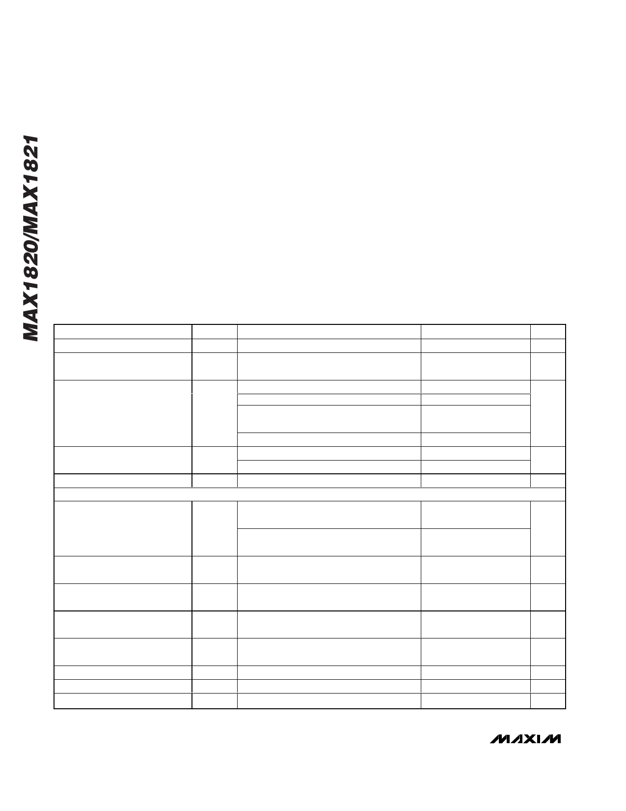
ELECTRICAL CHARACTERISTICS
(VBATT = 3.6V, SHDN = BATT, SKIP = SYNC = GND, VREF = 1.25V (MAX1820 only), TA = 0°C to +85°C, unless otherwise noted.
Typical values are at TA = +25°C.) (Note 2)
PARAMETER
Input BATT Voltage
Undervoltage Lockout
Threshold
Quiescent Current
Quiescent Current in Dropout
Shutdown Supply Current
ERROR AMPLIFIER
SYMBOL
VIN
CONDITIONS
VUVLO VBATT rising, 1% hysteresis
IQ
ISHDN
SKIP = GND (MAX1820Z/MAX1821)
SKIP = BATT, no switching
SKIP = GND (MAX1820Y, MAX1820X, and
MAX1821X)
SKIP = BATT, 1MHz switching
SKIP = GND
SKIP = BATT, no switching
SHDN = GND
MIN TYP MAX UNITS
2.6
5.5
V
2.20 2.35 2.55
V
180
300
450 2000
µA
240
360
3300
530 1000
µA
550 1000
0.1
6
µA
OUT Voltage Accuracy
(MAX1820)
VREF = 1.932 ±0.005V, load = 0 to 600mA,
SKIP = BATT or GND
3.33
3.4
3.47
VOUT
V
VREF = 0.227 ±0.005V, load = 0 to 30mA,
SKIP = BATT, VBATT ≤ 4.2V
0.35 0.40 0.45
OUT Input Resistance
(MAX1820)
ROUT
250 400
kΩ
REF Input Current (MAX1820)
IREF
0.1
1
µA
FB Voltage Accuracy
(MAX1821)
VFB
FB = COMP
1.225 1.25 1.275
V
FB Input Current (MAX1821)
Transconductance
COMP Clamp Low Voltage
COMP Clamp High Voltage
IFB
VFB = 1.4V
gm
0.01
50
nA
30
50
85
µS
0.2
0.45
1.0
V
2.04 2.15 2.28
V
2 _______________________________________________________________________________________
Share Link: 