MAX2106 データシートの表示(PDF) - Maxim Integrated
部品番号
コンポーネント説明
メーカー
MAX2106 Datasheet PDF : 10 Pages
| |||
DBS Direct Downconverter
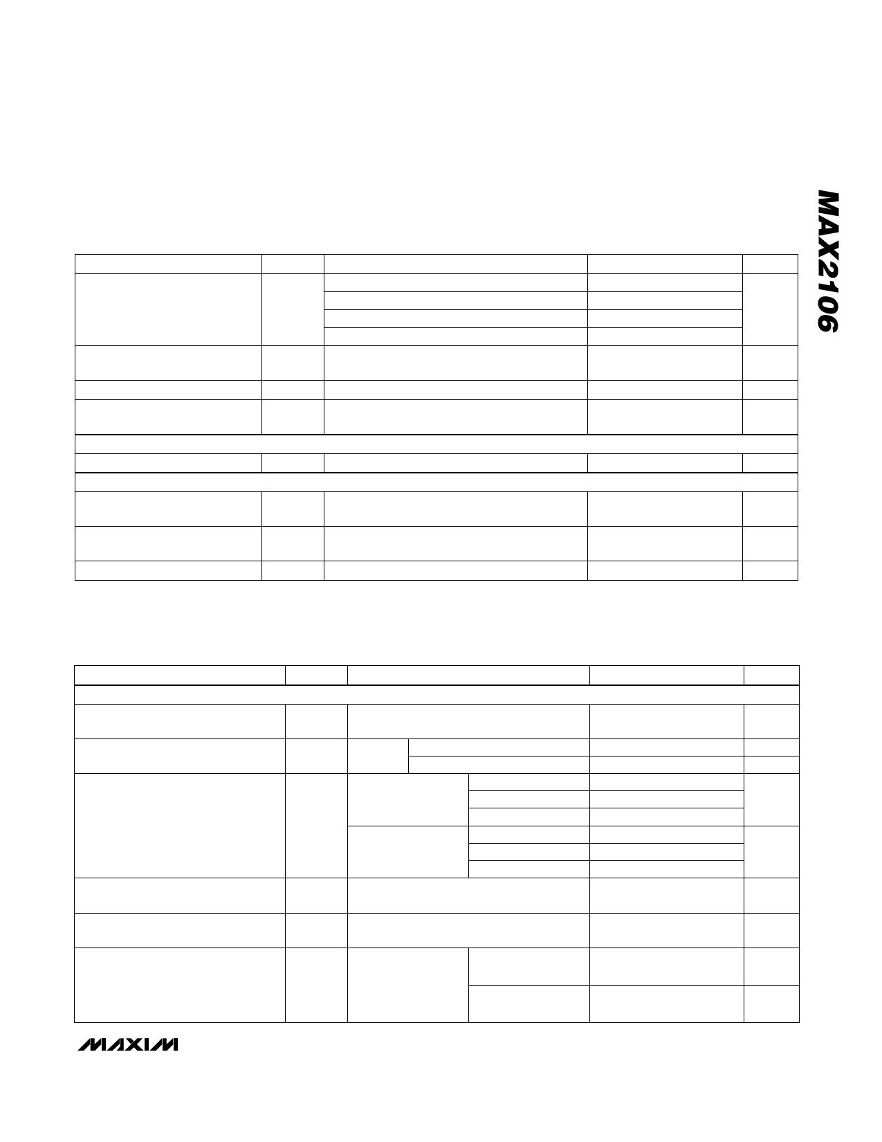
DC ELECTRICAL CHARACTERISTICS (continued)
(VCC = +4.75V to +5.25V, VFB = +2.4V, CIOUT_ = CQOUT_ = 10pF, ƒFLCLK = 2MHz, RFIN_ = unconnected, RIOUT_ = RQOUT_ = 10kΩ,
VLOBUFSEL = 0.5V, VRFBAND = VINSEL = VCPG1 = VCPG2 = +2.4V, VPLLIN+ = VMOD+ = +1.3V, VPLLIN- = VMOD- = +1.1V, TA = +25°C,
unless otherwise noted. Typical values are at VCC = +5V, unless otherwise noted.)
PARAMETER
SYMBOL
CONDITIONS
MIN TYP MAX UNITS
Charge-Pump Output Low
Measured at FB
VCPG1 ≤ 0.5V, VCPG2 ≤ 0.5V
VCPG1 ≤ 0.5V, VCPG2 ≥ 2.4V
VCPG1 ≥ 2.4V, VCPG2 ≤ 0.5V
VCPG1 ≥ 2.4V, VCPG2 ≥ 2.4V
-0.12 -0.1 -0.08
-0.36 -0.3 -0.24
mA
-0.72 -0.6 -0.48
-2.16 -1.8 -1.44
Charge-Pump Output Current
Matching Positive to Negative
Measured at FB
-5
5
%
Charge-Pump Output Leakage
Measured at FB
-25
25
nA
Charge-Pump Output Current
Drive (Note 1)
Measured at CP
100
µA
ANALOG CONTROL INPUTS (GC1, GC2)
Input Current
IGC_ VGC_ = 1V to 4V
-50
50
µA
BASEBAND OUTPUTS (IOUT+, IOUT-, QOUT+, QOUT-)
Differential Output Voltage
Swing
RL = 2kΩ differential
1
Vp-p
Common-Mode Output Voltage
(Note 1)
0.65
0.85
V
Offset Voltage (Note 1)
-50
50
mV
AC ELECTRICAL CHARACTERISTICS
(IC driven single-ended with RFIN- AC-terminated in 75Ω to GND, VCC = +4.75V to +5.25V, VIOUT_ = VQOUT_ = 0.59Vp-p,
CIOUT_ = CQOUT_ = 10pF, ƒLCLK = 2MHz, RIOUT_ = RQOUT_ = 10kΩ, VLOBUFSEL = 0.5V, VRFBAND = VINSEL = VCPG1 = VCPG2 = +2.4V,
VPLLIN+ = VMOD+ = +1.3V, VPLLIN- = VMOD- = +1.1V, TA = +25°C, unless otherwise noted. Typical values are at VCC = +5V.)
PARAMETER
SYMBOL
CONDITIONS
MIN
RF FRONT END
RFIN_ Input Frequency Range
fRFIN_
Inferred by quadrature gain and
phase-error test
925
RFIN_ Input Power for 0.59Vp-p
Single VGC1 = VGC2 = +4V (min gain) -25
Baseband Levels
carrier VGC1 = VGC2 = +1V (max gain)
RFIN_ Input Third-Order Intercept
Point (Note 3)
IP3RFIN_
PRFIN_ = -25dBm
per tone
PRFIN_ = -65dBm
per tone
fLO = 2175MHz
fLO = 1550MHz
fLO = 950MHz
fLO = 2175MHz
fLO = 1550MHz
fLO = 950MHz
RFIN_ Input Second-Order Intercept
(Note 4)
IP2RFIN_
PRFIN_ = -25dBm per tone,
fLO = 951MHz
Output-Referred 1dB Compression
Point (Note 5)
P1dBOUT
PRFIN_ = -40dBm,
signals within filter bandwidth
TYP
10.5
11.5
10.5
-29
-26
-30
17
2
MAX UNITS
2175
-68
MHz
dBm
dBm
dBm
dBm
dBm
dBV
Noise Figure
fRFIN_ = 1550MHz, PRFIN_ = -65dBm
NF
VGC1 = 1V, VGC2
adjusted 0.59Vp-p
baseband level
PRFIN_ = -25dBm
10.2
dB
44.8
dB
_______________________________________________________________________________________ 3
Share Link: 