MAX2108CEG データシートの表示(PDF) - Maxim Integrated
部品番号
コンポーネント説明
メーカー
MAX2108CEG Datasheet PDF : 12 Pages
| |||

Direct-Conversion Tuner IC
ABSOLUTE MAXIMUM RATINGS
VCC to GND ..............................................................-0.3V to +7V
VCC to Any Other VCC ...........................................-0.3V to +0.3V
All Other Pins to GND.................................-0.3V to (VCC + 0.3V)
RFIN to RFIN ..........................................................................±2V
LO to LO ................................................................................±2V
Short-Circuit Current
IOUT, IOUT, QOUT, QOUT to GND .................................10mA
PSOUT, PSOUT to GND...................................................40mA
Short-Circuit Duration IOUT to IOUT, QOUT to QOUT,
PSOUT to PSOUT ............................................................10sec
Continuous Power Dissipation (TA = +70°C)
24 QSOP (derate 10mW/°C above TA = +70°C) ..........800mW
Operating Temperature Range...............................0°C to +70°C
Junction Temperature ......................................................+150°C
Storage Temperature Range .............................-65°C to +150°C
Lead Temperature (soldering, 10s) .................................+300°C
Stresses beyond those listed under “Absolute Maximum Ratings” may cause permanent damage to the device. These are stress ratings only, and functional
operation of the device at these or any other conditions beyond those indicated in the operational sections of the specifications is not implied. Exposure to
absolute maximum rating conditions for extended periods may affect device reliability.
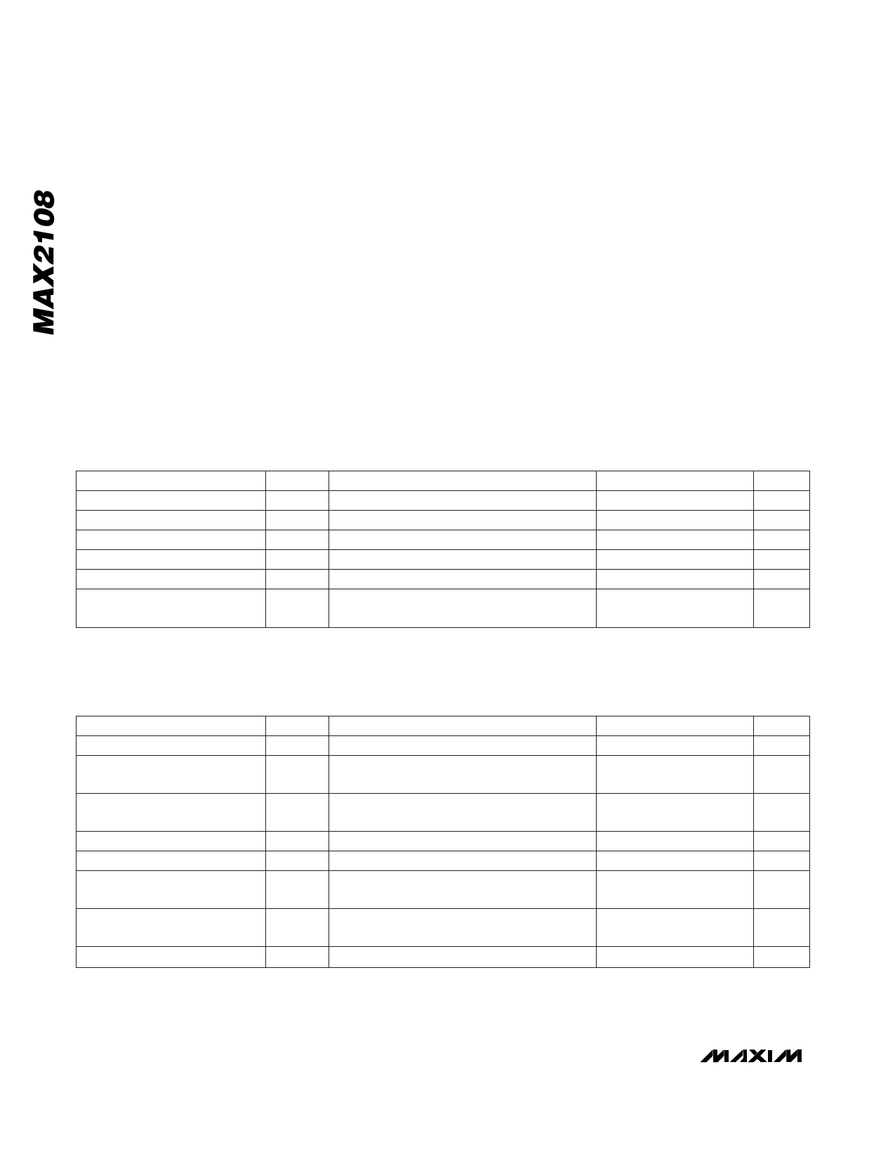
DC ELECTRICAL CHARACTERISTICS
(VCC = +4.75V to +5.25V; VGC = 1.3V; PS_SEL = 0.5V; IOUT, IOUT, QOUT, QOUT = terminated with 2.5kΩ to GND; no input signal
applied; TA = 0°C to +70°C; unless otherwise noted. Typical values are at VCC = +5V, TA = +25°C.)
PARAMETER
SYMBOL
CONDITIONS
MIN TYP MAX UNITS
Supply Current
ICC
105
152
mA
PS_SEL Logic-High Threshold
VTHH
2.4
V
PS_SEL Logic-Low Threshold
VTHL
0.5
V
PS_SEL Input Bias Current
IPS_SEL 0 < VPS_SEL < VCC
-30
+10
µA
GC Input Bias Current
IGC 1V < VGC < 4V
-80
+80
µA
IOUT, IOUT, QOUT, QOUT
Common-Mode Output Voltage
VCM
2.9
3.35
3.8
V
AC ELECTRICAL CHARACTERISTICS
(VCC = +5V; PS_SEL = 0.5V; PRFIN = -20dBm; fLO = fRFIN +125kHz; GC set via servo loop for VIOUT - V IOUT = 200mVp-p (differen-
tial); TA = +25°C; unless otherwise noted.)
PARAMETER
SYMBOL
CONDITIONS
MIN TYP MAX UNITS
RFIN Frequency Range (Note 1) fRFIN
950
2150 MHz
RFIN Maximum Input Power
(Note 2)
PRFINMAX 950MHz < fRFIN < 2150MHz, PLO = -5dBm
-20
dBm
RFIN Minimum Input Power
(Note 2)
External LO Drive Level (Note 2)
Gain-Control Range (Note 2)
RFIN Input Third-Order
Intercept Point (Note 3)
PRFINMIN
IIP3
950MHz < fRFIN < 2150MHz, PLO = -5dBm,
VIOUT - VIOUT = 10mVP-P, TA = 0°C +70°C
1V < VGC < 4V, PLO = -5dBm
-70 dBm
-5
50
dBm
dB
8
dBm
RFIN Input Second-Order
Intercept Point (Note 4)
IIP2
14
dBm
Noise Figure
NF VGC = 4V, fLO = 1750MHz
10
dB
2 _______________________________________________________________________________________