MAX2116(2005) データシートの表示(PDF) - Maxim Integrated
部品番号
コンポーネント説明
メーカー
MAX2116 Datasheet PDF : 15 Pages
| |||

Complete DBS Direct-Conversion Tuner ICs
with Monolithic VCOs
ABSOLUTE MAXIMUM RATINGS
VCC to GND ...........................................................-0.3V to +5.5V
All Other Pins to GND .................................-0.3V to (VCC + 0.3V)
RFIN+ to RFIN-, XTL+ to XTL-, IDC+ to IDC-,
QDC+ to QDC- ...................................................................±2.0V
CNTOUT, XTALOUT, CPOUT, VREG1/2,
I/QOUT± to GND Short-Circuit Duration.................................10s
Continuous Current (any pin other than VCC or GND) .......10mA
Continuous Power Dissipation (TA = +85°C)
40-Pin Thin QFN (derate 23.3mW/°C above +85°C) .... 1.86W
Operating Temperature Range ..............................0°C to +85°C
Junction Temperature .....................................................+150°C
Storage Temperature Range ............................-65°C to +160°C
Soldering Temperature (10s) ..........................................+300°C
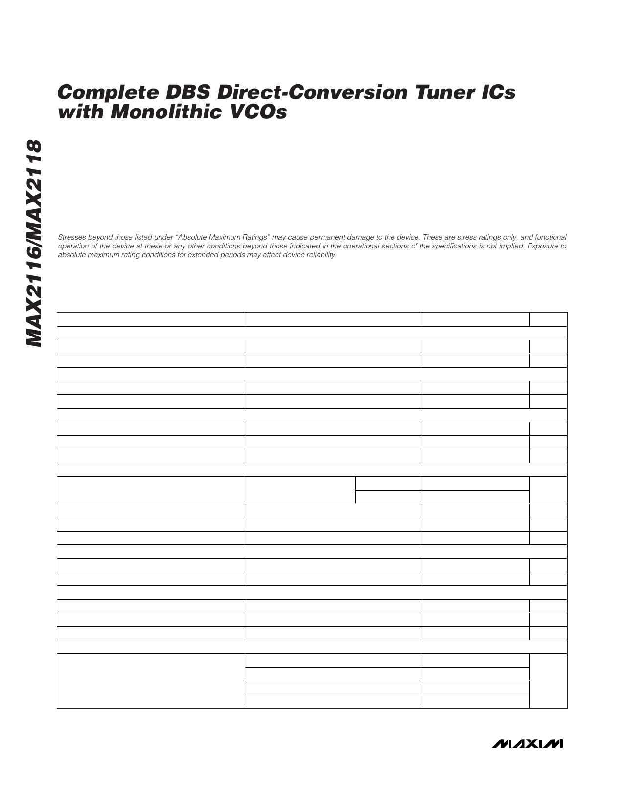
Stresses beyond those listed under “Absolute Maximum Ratings” may cause permanent damage to the device. These are stress ratings only, and functional
operation of the device at these or any other conditions beyond those indicated in the operational sections of the specifications is not implied. Exposure to
absolute maximum rating conditions for extended periods may affect device reliability.
DC ELECTRICAL CHARACTERISTICS
(VCC = +4.75V to +5.25V, GND = 0V, GC1 = +0.75V; no AC signal applied, default register settings, TA = 0°C to +85°C, unless other-
wise noted. Typical values are at VCC = +5V, TA = +25°C, unless otherwise noted.) (Note 1)
PARAMETER
CONDITIONS
SUPPLY
Supply Voltage
Supply Current
LO locked at 2175MHz
ANALOG GAIN CONTROL INPUT—GC1
Usable Voltage Range
Input Current
0.75V < GC1 < 2.6V (Note 2)
BASEBAND OUTPUTS— IOUT, QOUT (MAX2116)
Nominal Output Voltage Swing
Output Clipping Voltage
RLOAD = 1kΩ // 10pF (Note 3)
DC Output Voltage
BASEBAND OUTPUTS— IOUT±, QOUT± (MAX2118)
Nominal Output Voltage Swing
RLOAD = 2kΩ // 10pF
(differential) (Note 3)
Bit DL = high
Bit DL = low
Output Clipping Voltage
Common-Mode Voltage
DC Offset Voltage
ANALOG OUTPUT— VREG1, VREG2
Output Voltage
Source Current
Each output
STATIC CONTROL INPUTS—AS2, AS1, AS0
Input Voltage High
Input Voltage Low
Input Current
SYNTHESIZER DC PARAMETERS
Bits CP1 = 0, CP0 = 0
Charge Pump Source/Sink Current
Bits CP1 = 0, CP0 = 1
Bits CP1 = 1, CP0 = 0
Bits CP1 = 1, CP0 = 1
MIN TYP MAX UNITS
4.75
5.25
V
195 265
mA
0.75
2.6
V
-50
+50
µA
0.8
VP-P
2
VP-P
1.2
V
0.65
-50
1
0.59
2
0.75
0
0.85
+50
VP-P
VP-P
V
mV
2.7 2.85 3.05
V
3
mA
4
V
0.5
V
-50
+50
µA
±35
±50
±68
±70 ±100 ±136
µA
±140 ±200 ±272
±280 ±400 ±544
2 _______________________________________________________________________________________