MAX301CSE データシートの表示(PDF) - Maxim Integrated
部品番号
コンポーネント説明
メーカー
MAX301CSE Datasheet PDF : 8 Pages
| |||
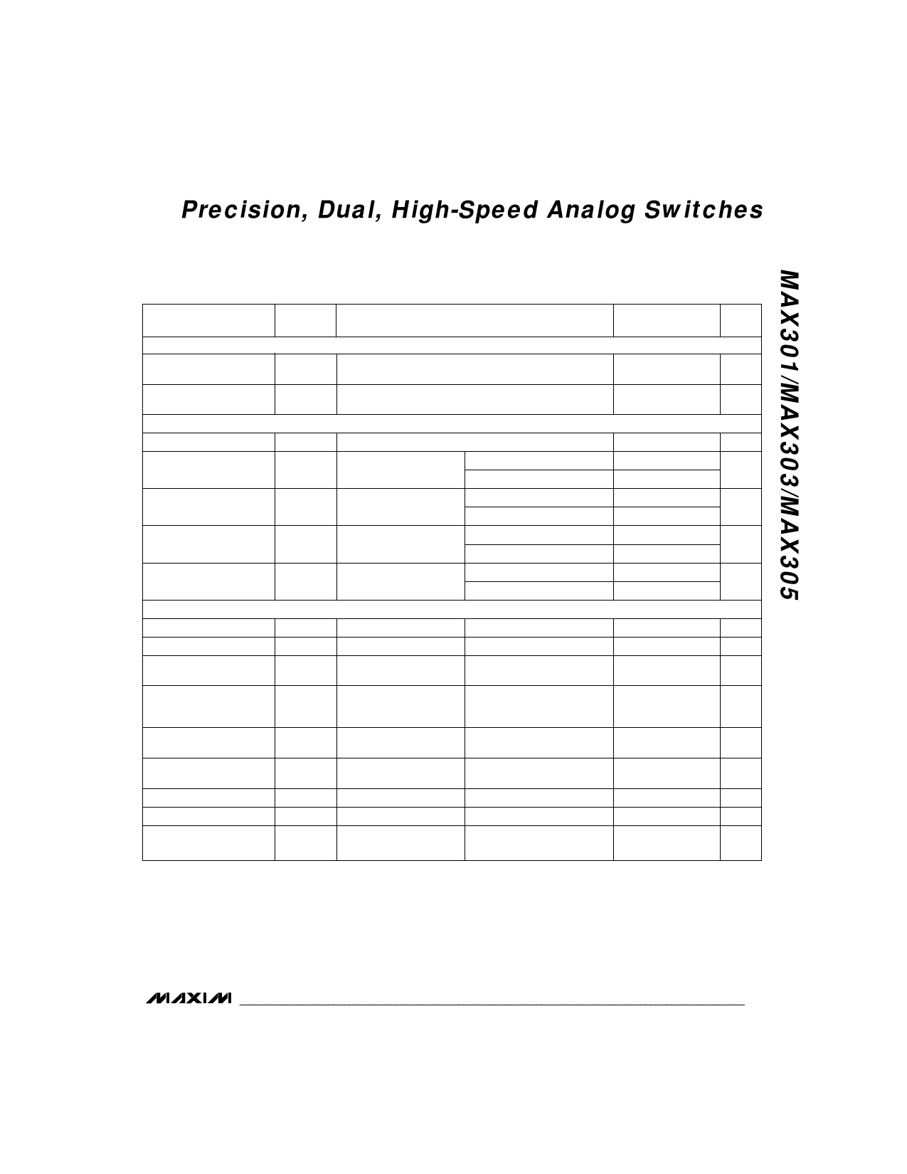
Precision, Dual, High-Speed Analog Switches
ELECTRICAL CHARACTERISTICS (continued)
(V+ = 15V, V- = -15V, VL = +5V, GND = 0V, VINH = +2.4V, VINL = +0.8V, TA = TMIN to TMAX, unless otherwise noted.)
PARAMETER
INPUT
Input Current with
Input Voltage High
Input Current with
Input Voltage Low
SUPPLY
Power-Supply Range
Positive Supply Current
Negative Supply Current
Logic Supply Current
Ground Current
DYNAMIC
Turn-On Time
Turn-Off Time
Break-Before-Make
Time Delay (Note 3)
Charge Injection
(Note 3)
Off Isolation (Note 5)
Crosstalk (Note 6)
Off Capacitance
COM Off Capacitance
SYMBOL
CONDITIONS
IINH
VIN_ = 2.4V, all others = 0.8V
IINH
VIN_ = 0.8V, all others = 2.4V
I+
I-
IL
IGND
All channels on or off,
VIN = 0V or 5V,
V+ = 16.5V, V- = -16.5V
All channels on or off,
VIN = 0V or 5V,
V+ = 16.5V, V- = -16.5V
All channels on or off,
VIN = 0V or 5V,
V+ = 16.5V, V- = -16.5V
All channels on or off,
VIN = 0V or 5V,
V+ = 16.5V, V- = -16.5V
TA = +25°C
TA = TMIN to TMAX
TA = +25°C
TA = TMIN to TMAX
TA = +25°C
TA = TMIN to TMAX
TA = +25°C
TA = TMIN to TMAX
tON
tOFF
tD
Q
OIRR
COFF
CCOM(OFF)
Figure1
Figure 1
MAX303 only,
Figure 2
CL = 10nF, VGEN = 0V,
RGEN = 0Ω,
Figure 3
RL = 100Ω, CL = 5pF,
f = 1MHz, Figure 4
RL = 50Ω, CL = 5pF,
f = 1MHz, Figure 5
f = 1MHz, Figure 6
f = 1MHz, Figure 6
TA = +25°C
TA = +25°C
TA = +25°C
TA = +25°C
TA = +25°C
TA = +25°C
TA = +25°C
TA = +25°C
MIN TYP MAX
(Note 2)
UNITS
-1.000 0.005 1.000 µA
-1.000 0.005 1.000 µA
±4.5
±20 V
-1.00 0.01 1.00
µA
-5.00
5.00
-1.00 -0.01 1.00
µA
-5.00
5.00
-1.00 0.01 1.00
µA
-5.00
5.00
-1.00 -0.01 1.00
µA
-5.00
5.00
100 150 ns
60 100 ns
10 20
ns
10 15 pC
72
dB
90
dB
12
pF
12
pF
Channel-On Capacitance CCOM(ON) f = 1MHz, Figure 7
TA = +25°C
39
pF
Note 2: The algebraic convention, where the most negative value is a minimum and the most positive value a maximum, is used on
this data sheet.
Note 3: Guaranteed by design.
Note 4: ∆RON = ∆RONMAX - ∆RONMIN. On resistance match between channels and flatness are guaranteed only with
specified voltages.
Note 5: See Figure 4. Off isolation = 20log10 VCOM/VNC orVNO, VCOM = output, VNC or VNO = input to off switch.
Note 6: Between any two switches. See Figure 5.
_________________________________________________________________________________________________ 3
Share Link: 