MAX3098EBCSE гғҮгғјгӮҝгӮ·гғјгғҲгҒ®иЎЁзӨәпјҲPDFпјү - Maxim Integrated
йғЁе“Ғз•ӘеҸ·
гӮігғігғқгғјгғҚгғігғҲиӘ¬жҳҺ
гғЎгғјгӮ«гғј
MAX3098EBCSE
Maxim Integrated

MAX3098EBCSE Datasheet PDF : 16 Pages
| |||
Вұ15kV ESD-Protected, 32Mbps, 3V/5V,
Triple RS-422/RS-485 Receivers with Fault Detection
Common-Mode Range
The MAX3097E/MAX3098E contain circuitry that de-
tects if the input stage is going outside its useful com-
mon-mode range. If the received data could be
unreliable, a fault signal is triggered.
Detecting Low Input Differential
Due to cable attenuation on long wire runs, it is possi-
ble that VID < 200mV, and incorrect data will be
received. In this condition, a fault will be indicated.
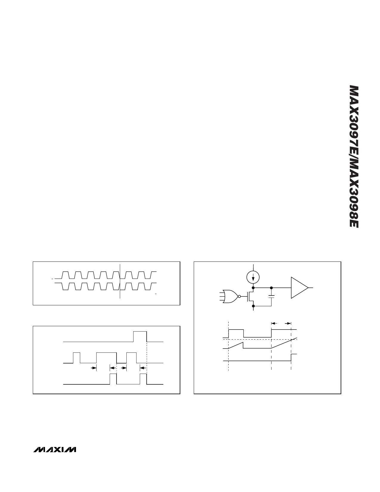
Delayed Fault Output
The delayed fault output provides a programmable
blanking delay to allow transient faults to occur without
triggering an alarm. Such faults may occur with slow
signals triggering the receiver alarm through the zero
crossover region.
Figure 9 shows the delayed alarm output.
ALARMD performs a logic OR of ALARMA, ALARMB,
and ALARMZ (Figure 10). A NOR gate drives an N-
channel MOSFET so that in normal operation with no
faults, the current source (10ВөA typ) is shunted to
ground. Upon activation of any alarm from receiver A,
B, or Z, the MOSFET is turned off, allowing the current
source to charge CDELAY. When VDELAY exceeds the
DELAY threshold, the comparator output, ALARMD,
goes high. ALARMD is reset when all receiver alarms
go low, quickly discharging CDELAY to ground.
Setting Delay Time
ALARMDвҖҷs delay time is set with a single capacitor
connected from DELAY to GND. The delay comparator
threshold varies with supply voltage, and the CDELAY
value can be determined for a given time delay period
from the Capacitance vs. ALARMD Output Delay graph
in the Typical Operating Characteristics or using the
following equations:
tD = 15 + 0.33 x CDELAY (for VCC = 5V)
and
tD = 10 + 0.187 x CDELAY (for VCC = 3V)
where tD is in Вөs and CDELAY is in pF.
A
A
NORMAL OPERATION
Figure 8. Short-Circuit Detection
SHORT CIRCUIT A TO A
ALARMA
ALARMB
ALARMD
tD
tD
Figure 9. Delayed Alarm Output
ALARMA
ALARMB
ALARMZ
ALARM_
DELAY
ALARMD
DELAY
CURRENT
SOURCE
NMOS
G1
CDELAY*
(EXTERNAL)
tDLY
DELAY
COMPARATOR
ALARMD
DELAY THRESHOLD
*The capacitor (CDELAY) charges up slowly, but discharges rapidly.
If the duration of an ALARM_ pulse is less than tDLY, no alarm
output will be present at ALARMD.
Figure 10. ALARMD Simplified Schematic
______________________________________________________________________________________ 11
Share Link: