MAX3097ECSE гғҮгғјгӮҝгӮ·гғјгғҲгҒ®иЎЁзӨәпјҲPDFпјү - Maxim Integrated
йғЁе“Ғз•ӘеҸ·
гӮігғігғқгғјгғҚгғігғҲиӘ¬жҳҺ
гғЎгғјгӮ«гғј
MAX3097ECSE
Maxim Integrated

MAX3097ECSE Datasheet PDF : 16 Pages
| |||
Вұ15kV ESD-Protected, 32Mbps, 3V/5V,
Triple RS-422/RS-485 Receivers with Fault Detection
ABSOLUTE MAXIMUM RATINGS
Supply Voltage (VCC).............................................................+7V
Receiver Input Voltage (A, A, B, B, Z, Z) .............................Вұ25V
Output Voltage (OUT_, ALARM_)...............-0.3V to (VCC + 0.3V)
DELAY ........................................................-0.3V to (VCC + 0.3V)
Continuous Power Dissipation (TA = +70В°C)
16-Pin QSOP (derate 8.3mW/В°C above +70В°C)............667mW
16-Pin SO (derate 8.7mW/В°C above +70В°C).................696mW
16-Pin Plastic DIP (derate 10.53mW/В°C
above +70В°C).............................................................762mW
Operating Temperature Ranges
MAX3097EC_E...................................................0В°C to +70В°C
MAX3098E_C_E .................................................0В°C to +70В°C
MAX3097E_E_E ..............................................-40В°C to +85В°C
MAX3098E_E_E ..............................................-40В°C to +85В°C
Storage Temperature Range .............................-65В°C to +150В°C
Junction Temperature ......................................................+150В°C
Lead Temperature (soldering, 10s) .................................+300В°C
Stresses beyond those listed under вҖңAbsolute Maximum RatingsвҖқ may cause permanent damage to the device. These are stress ratings only, and functional
operation of the device at these or any other conditions beyond those indicated in the operational sections of the specifications is not implied. Exposure to
absolute maximum rating conditions for extended periods may affect device reliability.
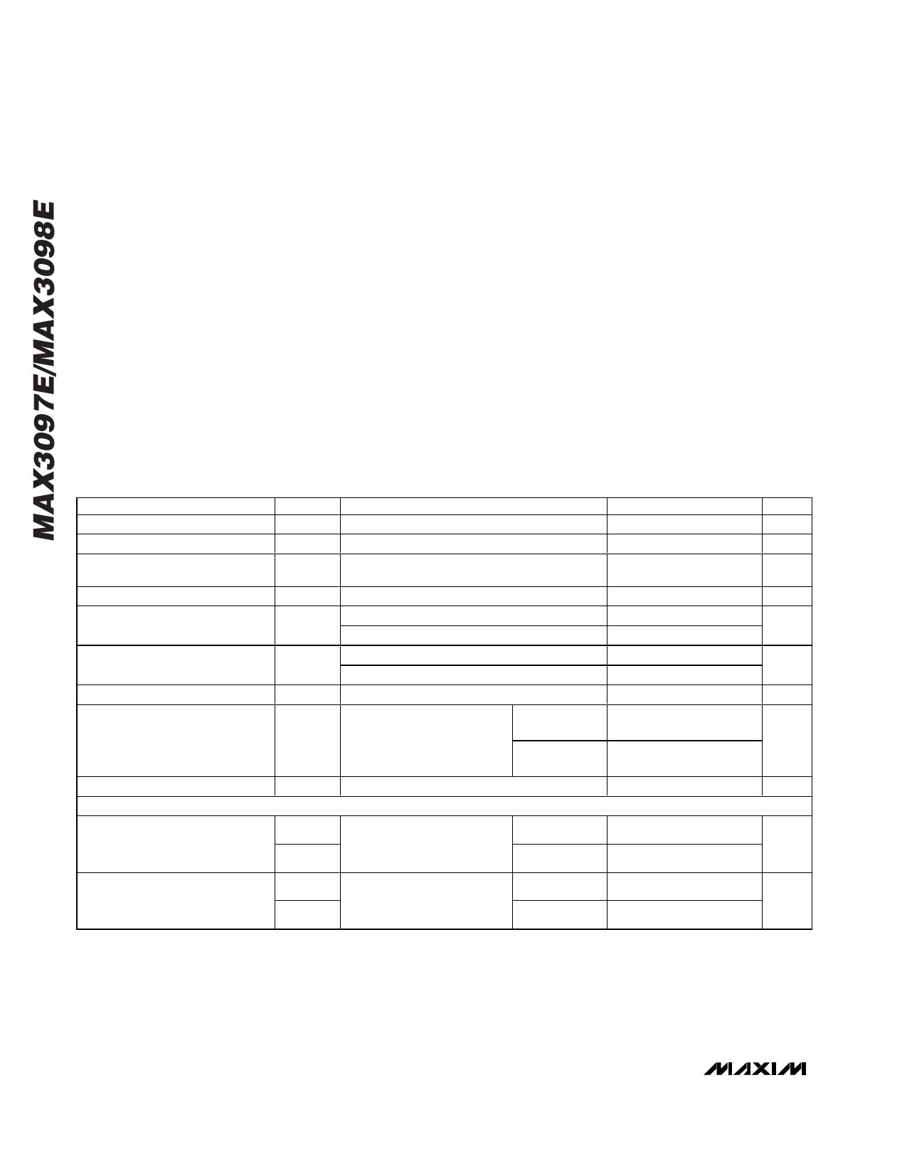
ELECTRICAL CHARACTERISTICS
(VCC = +3V to +5.5V, TA = TMIN to TMAX , unless otherwise noted. Typical values are at VCC = +5V and TA = +25В°C.)
PARAMETER
Supply Voltage Range
Supply Current
Receiver Differential Threshold
Voltage (Note 1)
Receiver Input Hysteresis
Output High Voltage
Output Low Voltage
Receiver Input Resistance
Input Current
(A , A , B , B (Z , Z )
Output Short-Circuit Current
FAULT DETECTION
SYMBOL
VCC
ICC
No load
CONDITIONS
VTH
-10V вүӨ VCM вүӨ 13.2V
вҲҶVTH
VOH
VOL
RIN
IIN
IOSR
-10V вүӨ VCM вүӨ 13.2V
VCC = 4.75V, IO = -4mA, VID = 200mV
VCC = 3.0V, IO = -1mA, VID = 200mV
VCC = 4.75V, IO = +4mA, VID = -200mV
VCC = 3.0V, IO = +1mA, VID = -200mV
-10V вүӨ VCM вүӨ 13.2V
VCC = 0 or 5.5V
VIN = 13.2V
(Note 2)
VIN = -10V
(Note 2)
0 вүӨ VRO вүӨ VCC
MIN TYP
3
3.1
-200
40
VCC - 1.5
VCC - 1.0
90
0.07
MAX
5.5
4.0
+200
0.4
0.4
160
0.14
-0.05
-0.11
Вұ105
MAX3097E Fault-Detection
Receiver Differential Threshold
Voltage (Note 3)
FDIFH
FDIFL
VCM = 0
High limit
Low limit
275
-475
475
-275
MAX3098EA Fault-Detection
Receiver Differential Threshold
Voltage (Note 3)
FDIFH
FDIFL
VCM = 0
High limit
Low limit
0.12
-0.20
0.20
-0.12
UNITS
V
mA
mV
mV
V
V
kв„Ұ
mA
mA
mV
V
2 _______________________________________________________________________________________
Share Link: