MAX351CSE データシートの表示(PDF) - Maxim Integrated
部品番号
コンポーネント説明
メーカー
MAX351CSE Datasheet PDF : 13 Pages
| |||
Precision, Quad, SPST Analog Switches
ABSOLUTE MAXIMUM RATINGS
Voltage Referenced to V-
V+ .......................................................................................44V
GND ...................................................................................25V
VL ................................................(GND - 0.3V) to (V+ + 0.3V)
Digital Inputs, VCOM, VNC, VNO (Note 1) ...........(V- - 2V) to (V+ + 2V)
.........................................................or 30mA (whichever occurs first)
Current (any terminal) .........................................................30mA
Peak Current COM_, NO_, NC_
(pulsed at 1ms, 10% duty cycle max) ..........................100mA
ESD per Method 3015.7 ..................................................>2000V
Continuous Power Dissipation (TA = +70°C) (Note 2)
Plastic DIP (derate 10.53mW/°C above +70°C) ..........842mW
Narrow SO (derate 8.70mW/°C above +70°C) ............696mW
QFN (derate 19.2mW/°C above +70°C) ....................1538mW
CERDIP (derate 10.00mW/°C above +70°C) ...............800mW
Operating Temperature Ranges:
MAX35_C_ _ .......................................................0°C to +70°C
MAX35_E_ _.....................................................-40°C to +85°C
MAX35_MJE ..................................................-55°C to +125°C
Storage Temperature Range .............................-65°C to +150°C
Lead Temperature (soldering, 10s) .................................+300°C
Note 1: Signals on NC_, NO_, COM_, or IN_ exceeding V+ or V- will be clamped by internal diodes. Limit forward diode current to
maximum current rating.
Note 2: All leads are soldered or welded to PC board.
Stresses beyond those listed under “Absolute Maximum Ratings” may cause permanent damage to the device. These are stress ratings only, and functional
operation of the device at these or any other conditions beyond those indicated in the operational sections of the specifications is not implied. Exposure to
absolute maximum rating conditions for extended periods may affect device reliability.
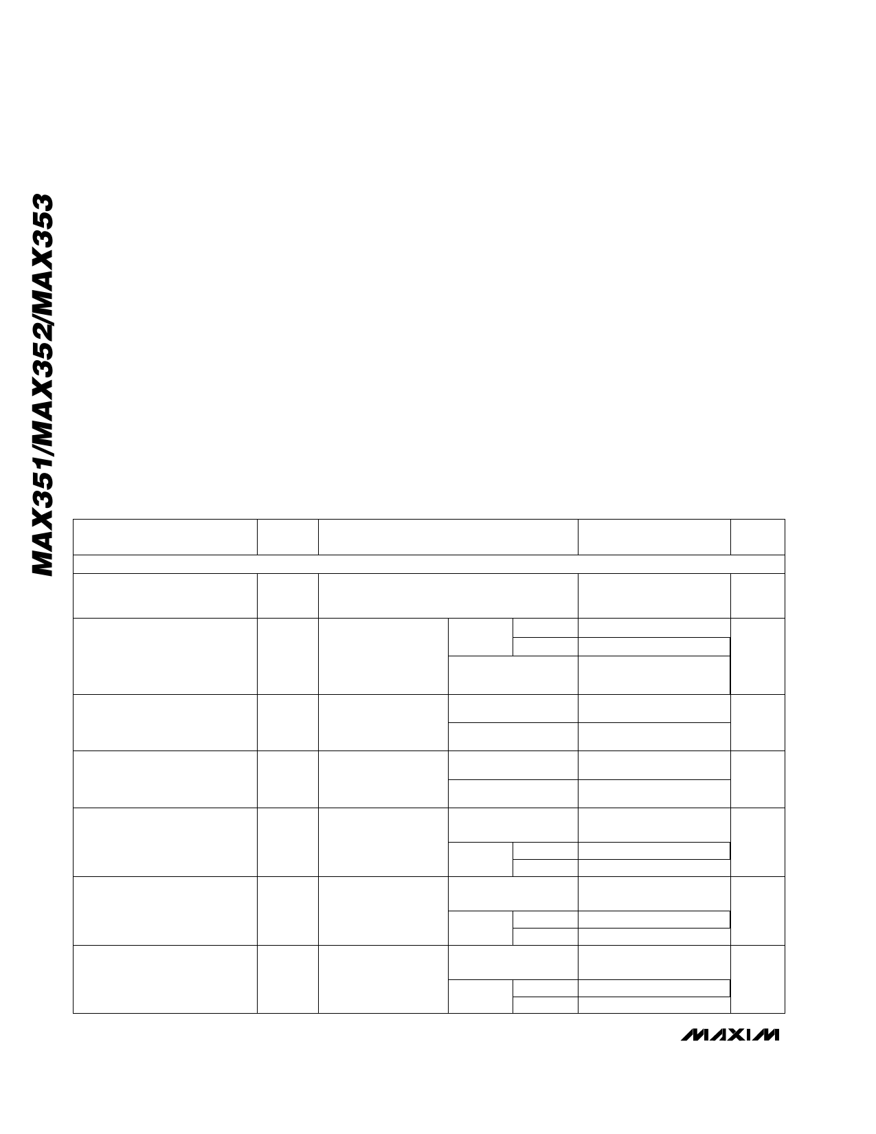
ELECTRICAL CHARACTERISTICS—Dual Supplies
(V+ = 15V, V- = -15V, VL = 5V, GND = 0V, VINH = 2.4V, VINL = 0.8V, TA = TMIN to TMAX, unless otherwise noted.)
PARAMETER
SYMBOL
CONDITIONS
MIN TYP
(Note 3)
SWITCH
Analog Signal Range
On Resistance
VCOM_,
VNO_,
VNC_
RON
(Notes 1, 4)
ICOM = -10mA,
VNO_ or VNC_ = ±8.5V,
V+ = 13.5V,
V- = -13.5V
TA =
C, E
+25°C
M
TA = TMIN to TMAX
V-
17
17
MAX
V+
35
30
45
UNITS
V
Ω
On Resistance Match Between
Channels (Note 5)
RON
ICOM = -10mA,
TA = +25°C
VNO_ or VNC_ = ±10V,
V+ = 15V, V- = - 15V TA = TMIN to TMAX
On Resistance Flatness (Note 5) RON
ICOM = -10mA,
VNO_ or VNC_ = ±5V,
V+ = 15V, V- = - 15V
TA = +25°C
TA = TMIN to TMAX
Off Leakage Current
(NO_ or NC_)
COM_ Off Leakage Current
COM_ On Leakage Current
VCOM = -15.5V,
TA = +25°C
INO
VNO_ or VNC_ = 15.5V,
INC
V+ = 16.5V,
V- = -16.5V
TA = TMIN C, E
to TMAX M
INC(OFF)
VCOM = -15.5V,
VNO_ or VNC_ = 15.5V,
V+ = 16.5V,
V- = -16.5V
TA = +25°C
TA = TMIN C, E
to TMAX M
ICOM(ON)
VCOM = ±15.5V,
VNO_ or VNC_ = ±15.5V,
V+ = 16.5V,
V- = -16.5V
TA = +25°C
TA = TMIN C, E
to TMAX M
2
Ω
4
3
Ω
5
-0.25 -0.10 0.25
nA
-6
6
-20
20
-0.25 -0.10 0.25
nA
-6
6
-20
20
-0.4
-0.1
0.4
nA
-10
10
-40
40
2 _______________________________________________________________________________________
Share Link: 