MAX3760(1998) データシートの表示(PDF) - Maxim Integrated
部品番号
コンポーネント説明
メーカー
MAX3760
(Rev.:1998)
(Rev.:1998)
Maxim Integrated

MAX3760 Datasheet PDF : 8 Pages
| |||
622Mbps, Low-Noise Transimpedance
Preamplifier for LAN and WAN Optical Receivers
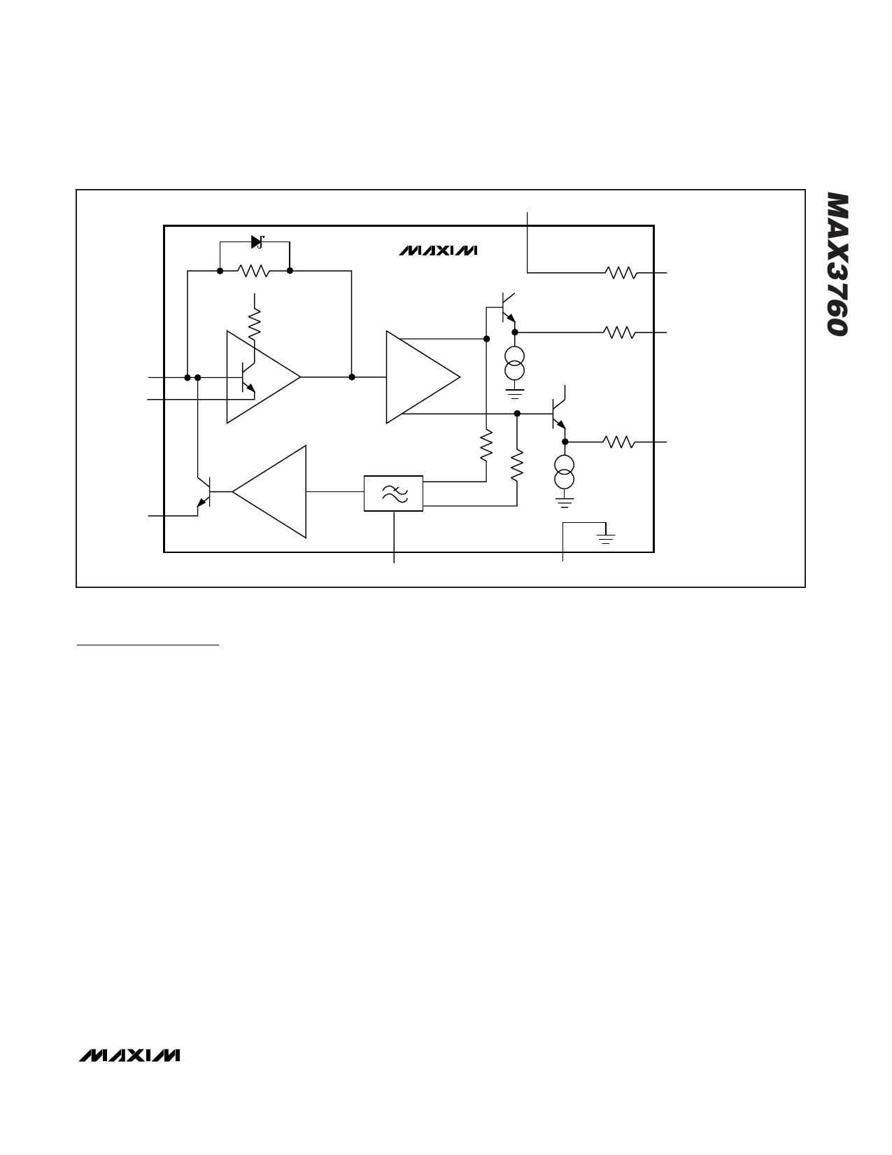
IN
INREF
D1
RF
VCC
TRANSIMPEDANCE
AMPLIFIER
Q1
Q4
GND
DC
CANCELLATION
AMPLIFIER
VCC
1k
MAX3760
VCC
Q2
R1
PARAPHASE
AMP
R3
VCC
Q3
R2
R4
(FILTER)
OUT-
OUT+
COMP
Figure 1. Functional Diagram
Detailed Description
The MAX3760 is a transimpedance amplifier designed
for 622Mbps fiber optic applications. As shown in the
Functional Diagram (Figure 1), it comprises a transim-
pedance amplifier, a paraphase amplifier with emitter-
follower outputs, and a DC cancellation circuit.
Transimpedance Amplifier
The signal current at the input flows into a high-gain
amplifier’s summing node. Shunt feedback through RF
converts this current to a voltage with 6.5kΩ gain.
Diode D1 clamps the output voltage for large input cur-
rents. INREF is a direct connection to the input transis-
tor’s emitter, and must be connected directly to the
photodetector AC ground return for best performance.
Paraphase Amplifier
The paraphase amplifier converts single-ended signals to
differential signals and introduces a voltage gain of 2.
This signal drives a pair of internally biased emitter follow-
ers, Q2 and Q3, which form the output stage. Resistors
R1 and R2 provide back-termination at the output, deliv-
ering a 100Ω differential output impedance. The output
emitter followers are designed to drive a 100Ω differential
load between OUT+ and OUT-. The MAX3760 can also
GND
( ) INDICATE PINS AVAILABLE ON DIE ONLY.
be terminated with higher output impedances for
increased gain and output voltage swing. The MAX3760
will not drive a 50Ω load to ground. For best noise rejec-
tion, terminate the MAX3760 with differential loads.
DC Cancellation Circuit
The DC cancellation circuit removes the input signal’s
DC component by employing low-frequency feedback.
This feature centers the input signal within the transim-
pedance amplifier’s dynamic range, thereby reducing
pulse-width distortion on large input signals.
The paraphase amplifier’s output is sensed through
resistors R3 and R4, then filtered, amplified, and fed
back to the base of transistor Q4. The transistor draws
the input signal’s DC component away from the trans-
impedance amplifier’s summing node.
The MAX3760 DC cancellation loop is internally com-
pensated and does not require external capacitors in
most 622Mbps applications. Add external capacitance
at the COMP pin to reduce the DC cancellation circuit’s
frequency response and improve data-dependent jitter.
Connecting the COMP pin directly to GND disables the
circuit. The DC cancellation circuit can sink up to 1mA
at the input.
_______________________________________________________________________________________ 5
Share Link: