MAX3622 データシートの表示(PDF) - Maxim Integrated
部品番号
コンポーネント説明
メーカー
MAX3622 Datasheet PDF : 9 Pages
| |||
Low-Jitter, Precision Clock Generator
with Two Outputs
ELECTRICAL CHARACTERISTICS (continued)
(VCC = +3.0V to +3.6V, TA = 0°C to +70°C, unless otherwise noted. Typical values are at VCC = +3.3V, TA = +25°C, unless otherwise
noted.) (Notes 1, 2)
PARAMETER
SYMBOL
CLOCK OUTPUT AC SPECIFICATIONS
VCO Frequency Range
Random Jitter
RJRMS
CONDITIONS
12kHz to 20MHz
1.875MHz to 20MHz
MIN TYP MAX UNITS
620
625
648
MHz
0.36
0.14
1.0
psRMS
Deterministic Jitter Induced by
Power-Supply Noise
(Notes 5, 6)
LVPECL output
LVCMOS output
4
psP-P
19
Spurs Induced by Power-Supply
Noise (Note 6)
LVPECL output
LVCMOS output
-57
dBc
-47
Nonharmonic and Subharmonic
Spurs
-70
dBc
f = 1kHz
-124
Clock Output SSB Phase Noise
at 125MHz
f = 10kHz
f = 100kHz
f = 1MHz
-126
-130
-145
dBc/H z
f > 10MHz
-153
Note 1:
Note 2:
Note 3:
Note 4:
Note 5:
Note 6:
A series resistor of up to 10.5Ω is allowed between VCC and VCCA for filtering supply noise when system power-supply
tolerance is VCC = 3.3V ±5%. See Figure 2.
LVPECL terminated with 50Ω load connected to VTT = VCC - 2V.
Both outputs enabled and unloaded.
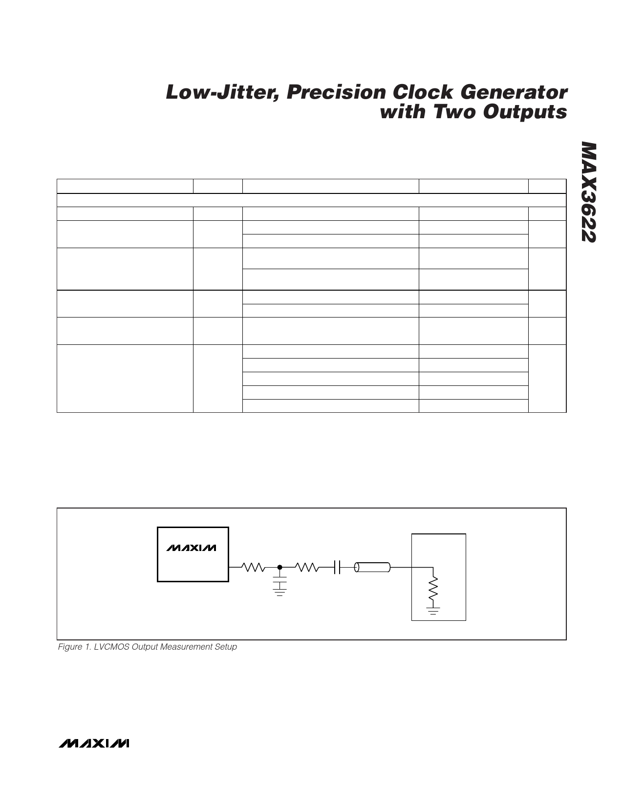
Measured using setup shown in Figure 1 with VCC = 3.3V ±5%.
Measured with Agilent DSO81304A 40GS/s real-time oscilloscope.
Measured with 40mVP-P, 100kHz sinusoidal signal on the supply with VCCA connected as shown in Figure 2.
MAX3622
36Ω
QA_C
499Ω 0.1μF
4.7pF
Z0 = 50Ω
OSCILLOSCOPE
50Ω
Figure 1. LVCMOS Output Measurement Setup
_______________________________________________________________________________________ 3
Share Link: 