MAX4508CSE(2007) データシートの表示(PDF) - Maxim Integrated
部品番号
コンポーネント説明
メーカー
MAX4508CSE
(Rev.:2007)
(Rev.:2007)
Maxim Integrated

MAX4508CSE Datasheet PDF : 18 Pages
| |||
Fault-Protected, High-Voltage Single 8-to-1/
Dual 4-to-1 Multiplexers with Output Clamps
NORMALLY OPEN SWITCH CONSTRUCTION
V+
P2
HIGH
FAULT
NO_
LOW
FAULT
P1
N1
COM_
A-
ON
GWD
MAX4508
MAX4509
V-
N2
ESO CODE
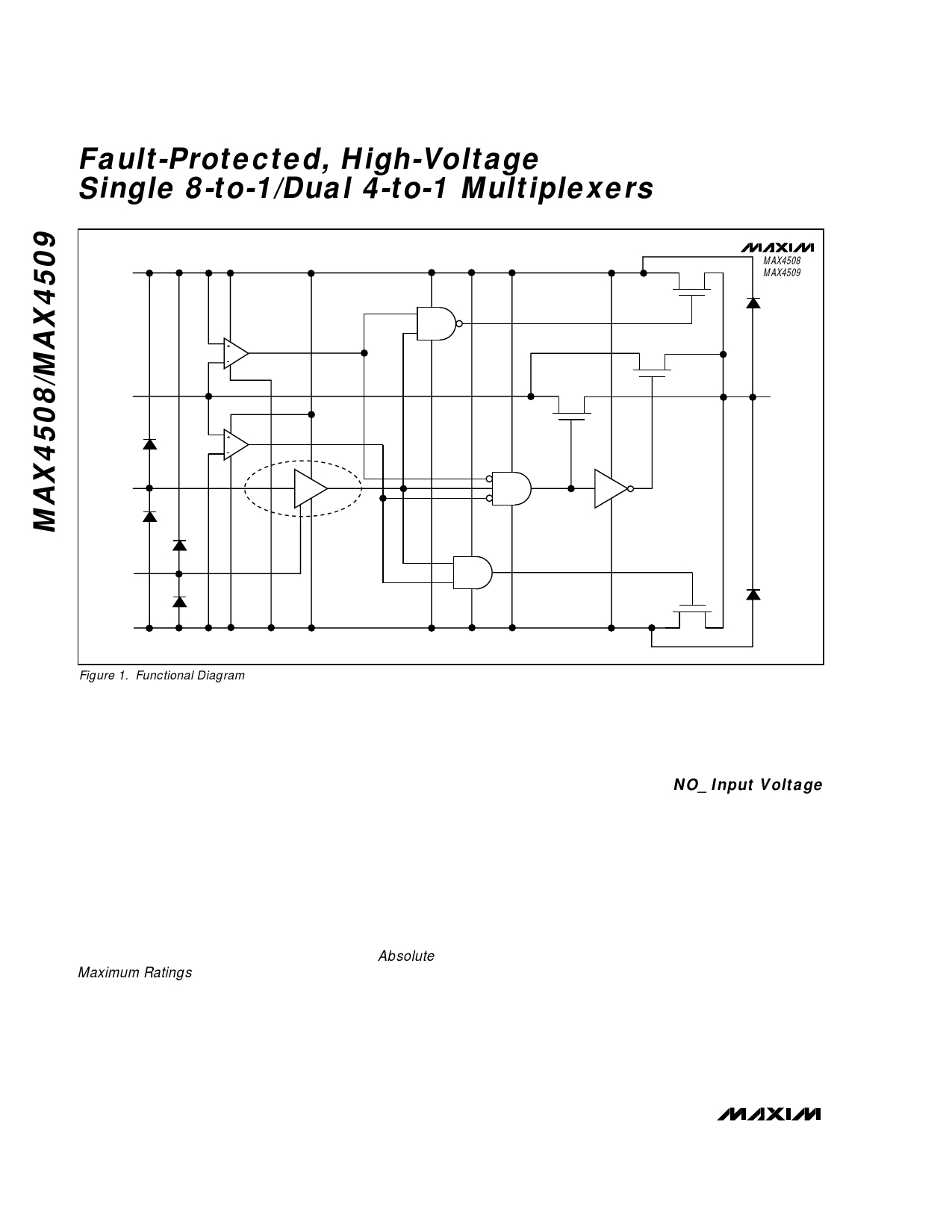
Figure 1. Functional Diagram
When the NO_ voltage goes beyond supply rails (fault
condition), the NO_ input becomes high impedance
regardless of the switch state or load resistance. When
power is removed, and the fault protection is still in
effect, the NO_ terminals are a virtual open circuit. The
fault can be up to ±40V, with V+ = V- = 0. If the switch
is on, the COM_ output current is furnished from the V+
or V- pin by “booster” FETs connected to each supply
pin. These FETs can source or sink up to 10mA.
The COM_ pins are not fault protected. If a voltage
source is connected to any COM_ pin, it should be lim-
ited to the supply voltages. Exceeding the supply volt-
age will cause high currents to flow through the ESD
protection diodes, damaging the device (see Absolute
Maximum Ratings).
Figure 1 shows the internal construction, with the ana-
log signal paths shown in bold. A single normally open
(NO) switch is shown. The analog switch is formed by
the parallel combination of N-channel FET N1 and P-
channel FET P1, which are driven on and off simultane-
ously, according to the input fault condition and the
logic level state.
NO_ Input Voltage
The maximum allowable input voltage for safe opera-
tion depends on whether supplies are on or off and the
load configuration at the COM output. If COM is re-
ferred to a voltage other than ground, but within the
supplies, VNO_ may range higher or lower than the sup-
plies provided the absolute value of ⎢VNO_ - VCOM_⎢ is
less than 40V. For example, if the load is referred to
+10V at COM_, then the NO_ voltage range can be
from +50V to -30V. As another example, if the load is
connected to -10V at COM_, the NO_ voltage range is
limited to -50V to +30V.
If the supplies are ±15V and COM is referenced to
ground through a load, the maximum NO_ voltage is
±25V. If the supplies are off and the COM output is ref-
erenced to ground, the maximum NO_ voltage is ±40V.
Normal Operation
Two comparators continuously compare the voltage on
the NO_ pin with V+ and V- supply voltages. When the
signal on NO_ is between V+ and V-, the multiplexer
behaves normally, with FETs N1 and P1 turning on and
off in response to A_ signals (Figure 1). The parallel
10 ______________________________________________________________________________________
Share Link: