MAX4508CSE データシートの表示(PDF) - Maxim Integrated
部品番号
コンポーネント説明
メーカー
MAX4508CSE Datasheet PDF : 16 Pages
| |||
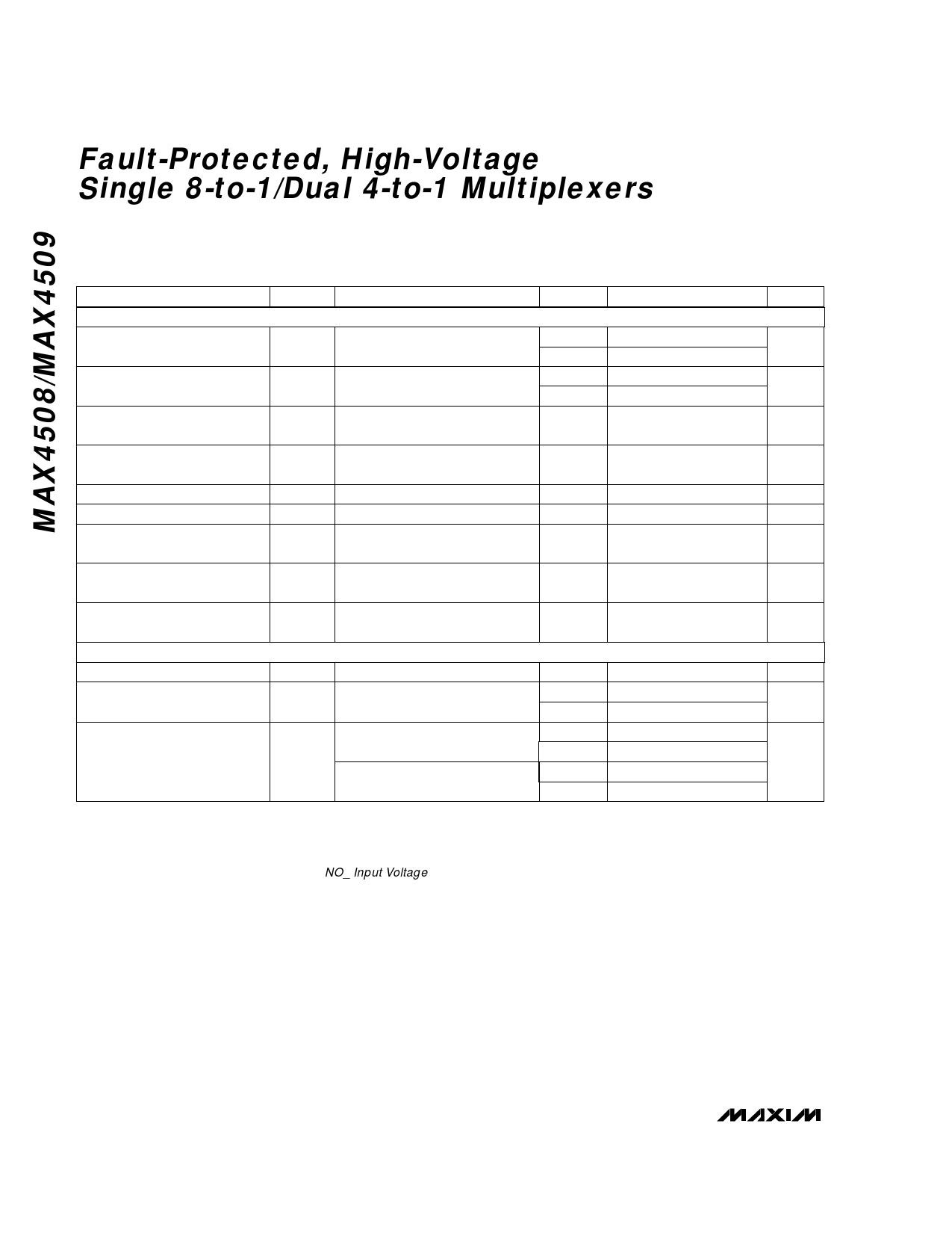
Fault-Protected, High-Voltage
Single 8-to-1/Dual 4-to-1 Multiplexers
ELECTRICAL CHARACTERISTICS—Single +12V Supply (continued)
(V+ = +12V, V- = 0, VA_H = +2.4V, VA_L = +0.8V, VEN = +2.4V, TA = TMIN to TMAX, unless otherwise noted. Typical values are at
TA = +25°C.) (Note 2)
PARAMETER
SYMBOL
CONDITIONS
SWITCH DYNAMIC CHARACTERISTICS
Enable Turn-On Time
tON
VCOM_ = 10V, RL = 2kΩ,
Figure 3
Enable Turn-Off Time
tOFF
VCOM_ = 10V, RL = 2kΩ,
Figure 3
Break-Before-Make Time Delay
(Note 4)
tBBM
VCOM_ = 10V, RL = 2kΩ,
Figure 4
TA
MIN TYP MAX UNITS
+25°C
C, E, M
+25°C
C, E, M
220
500
ns
700
100
250
ns
350
+25°C
50
100
ns
Charge Injection
(Note 4)
Q
CL = 1.0nF, VNO_ = 0, RS = 0,
Figure 5
+25°C
2
10
pC
NO_ Off-Capacitance
CNO_(OFF) VNO_ = 0, f = 1MHz, Figure 8
+25°C
10
pF
COM_ Off-Capacitance
CCOM_(OFF) VCOM_ = 0, f = 1MHz, Figure 8
+25°C
19
pF
COM_ On-Capacitance
CCOM_(ON)
VCOM_ = VNO_ = 0, f = 1MHz,
Figure 8
+25°C
28
pF
Off-Isolation
(Note 7)
VISO
RL = 75Ω, CL = 15pF,
VNO_ = 1VRMS, f = 1MHz, Figure 6
+25°C
-70
dB
Channel-to-Channel Crosstalk
(Note 8)
VCT
RL = 75Ω, CL = 15pF,
VNO_ = 1VRMS, f = 1MHz, Figure 7
+25°C
-62
dB
POWER SUPPLY
Power-Supply Range
V+
C, E, M
9
36
V
V+ Supply Current
I+
All VA_ = 0 or 5V,
VNO_ = 0, VEN = 5V
+25°C
C, E, M
200
300
µA
450
V- and GND Supply Current
IGND
All VA_ = 0 or 5V,
VNO_ = 0, VEN = +5V
All VA_ = 0 or 5V
+25°C
C, E, M
+25°C
C, E, M
150
250
375
µA
250
400
600
Note 2: The algebraic convention is used in this data sheet; the most negative value is shown in the minimum column.
Note 3: NO_ pins are fault protected and COM_ pins are not fault protected. The max input voltage on NO_ pins depends on the
COM_ load configuration. Generally the max input voltage is ±36V with ±15V supplies and a load referred to ground. For
more detailed information refer to NO_ Input Voltage section.
Note 4: Guaranteed by design.
Note 5: ∆RON = RON(MAX) - RON(MIN).
Note 6: Leakage parameters are 100% tested at the maximum rated hot temperature and guaranteed by correlation at TA = +25°C.
Note 7: Off-isolation = 20log10 (VCOM_ / VNO_ ), where VCOM_ = output and VNO_ = input to off switch.
Note 8: Between any two analog inputs.
Note 9: Leakage testing for single-supply operation is guaranteed by testing with dual supplies.
Note 10: Guaranteed by testing with dual supplies.
6 _______________________________________________________________________________________
Share Link: 