MAX4547CSE データシートの表示(PDF) - Maxim Integrated
部品番号
コンポーネント説明
メーカー
MAX4547CSE Datasheet PDF : 16 Pages
| |||
Quad/Dual, Low-Voltage,
Bidirectional RF/Video Switches
______________________________________________________________Pin Description
MAX4545
PIN
MAX4546
MAX4547
NAME
1, 10, 11,
20
1, 16
1, 9
IN_
3, 6, 8, 13,
15, 18
3, 7, 10, 14 4, 6, 12, 14
GND_
16
12
7, 15
V+
5
5
3, 11
V-
4, 7, 14, 17
—
2, 9, 12, 19
4, 13
6, 11
2, 8, 9, 15
2, 16
8, 10
5, 13
NO_
NC_
COM_
FUNCTION*
Digital Control Input
RF and Logic Ground. Grounds are not internally connected to each other,
and should all be connected to a ground plane (see Grounding section).
Positive Supply-Voltage Input (analog and digital)
Negative Supply-Voltage Input. Connect to ground plane for single-supply
operation.
Analog Switch Normally Open** Terminals
Analog Switch Normally Closed** Terminals
Analog Switch Common** Terminals
* All pins have ESD diodes to V- and V+.
** NO_ (or NC_) and COM_ pins are identical and interchangeable. Either may be considered as an input or output; signals pass
equally well in either direction.
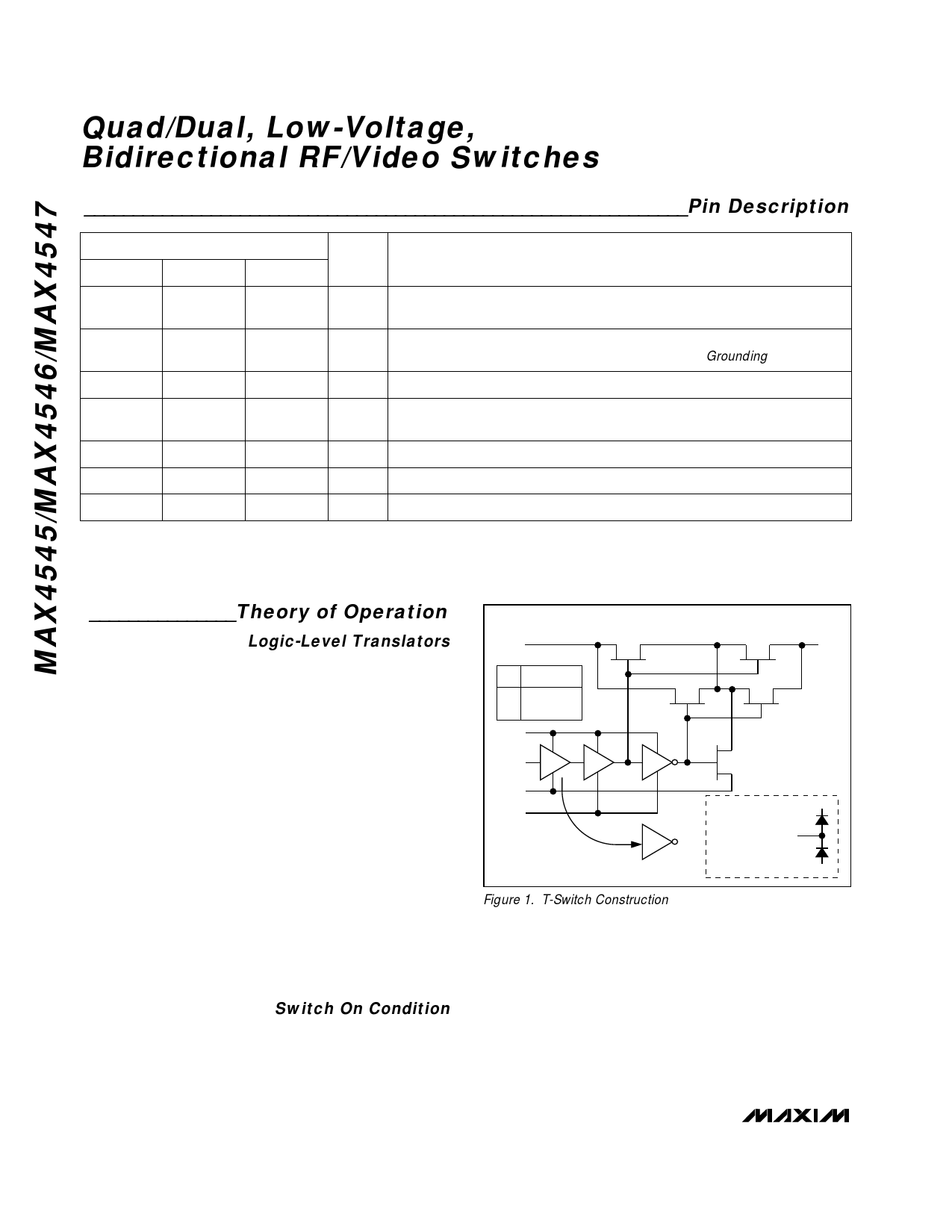
_______________Theory of Operation
Logic-Level Translators
The MAX4545/MAX4546/MAX4547 are constructed as
high-frequency “T” switches, as shown in Figure 1. The
logic-level input, IN_, is translated by amplifier A1 into a
V+ to V- logic signal that drives amplifier A2. (Amplifier
A2 is an inverter for normally closed switches.)
Amplifier A2 drives the gates of N-channel MOSFETs
N1 and N2 from V+ to V-, turning them fully on or off.
The same signal drives inverter A3 (which drives the
P-channel MOSFETs P1 and P2) from V+ to V-, turning
them fully on or off, and drives the N-channel MOSFET
N3 off and on.
The logic-level threshold is determined by V+ and
GND_. The voltage on GND_ is usually at ground
potential, but it may be set to any voltage between
(V+ - 2V) and V-. When the voltage between V+ and
GND_ is less than 2V, the level translators become very
slow and unreliable. Since individual switches in each
package have individual GND_ pins, they may be set to
different voltages. Normally, however, they should all
be connected to the ground plane.
Switch On Condition
When the switch is on, MOSFETs N1, N2, P1, and P2
are on and MOSFET N3 is off. The signal path is COM_
to NO_, and because both N-channel and P-channel
MOSFETs act as pure resistances, it is symmetrical
NORMALLY OPEN SWITCH CONSTRUCTION
COM_
IN_ COM_ - NO_
0
OFF
1
ON
N1
D
S
N2
D
S
P1
S
D
P2
S
D
V+
IN_
GND_
V-
A1
A2
D
A3
N3
S
A1
(NC)
BSD DIODES
ON GND_, IN_,
COM_, NO_, AND NC_
NO_
V+
V+
Figure 1. T-Switch Construction
(i.e., signals may pass in either direction). The off
MOSFET, N3, has no DC conduction, but has a small
amount of capacitance to GND_. The four on
MOSFETs also have capacitance to ground that,
together with the series resistance, forms a lowpass fil-
ter. All of these capacitances are distributed evenly
along the series resistance, so they act as a transmis-
sion line rather than a simple R-C filter. This helps to
explain the exceptional 300MHz bandwidth when the
switches are on.
8 _______________________________________________________________________________________
Share Link: 