MAX4552CSE гғҮгғјгӮҝгӮ·гғјгғҲгҒ®иЎЁзӨәпјҲPDFпјү - Maxim Integrated
йғЁе“Ғз•ӘеҸ·
гӮігғігғқгғјгғҚгғігғҲиӘ¬жҳҺ
гғЎгғјгӮ«гғј
MAX4552CSE Datasheet PDF : 16 Pages
| |||
Вұ15kV ESD-Protected, Quad,
Low-Voltage, SPST Analog Switches
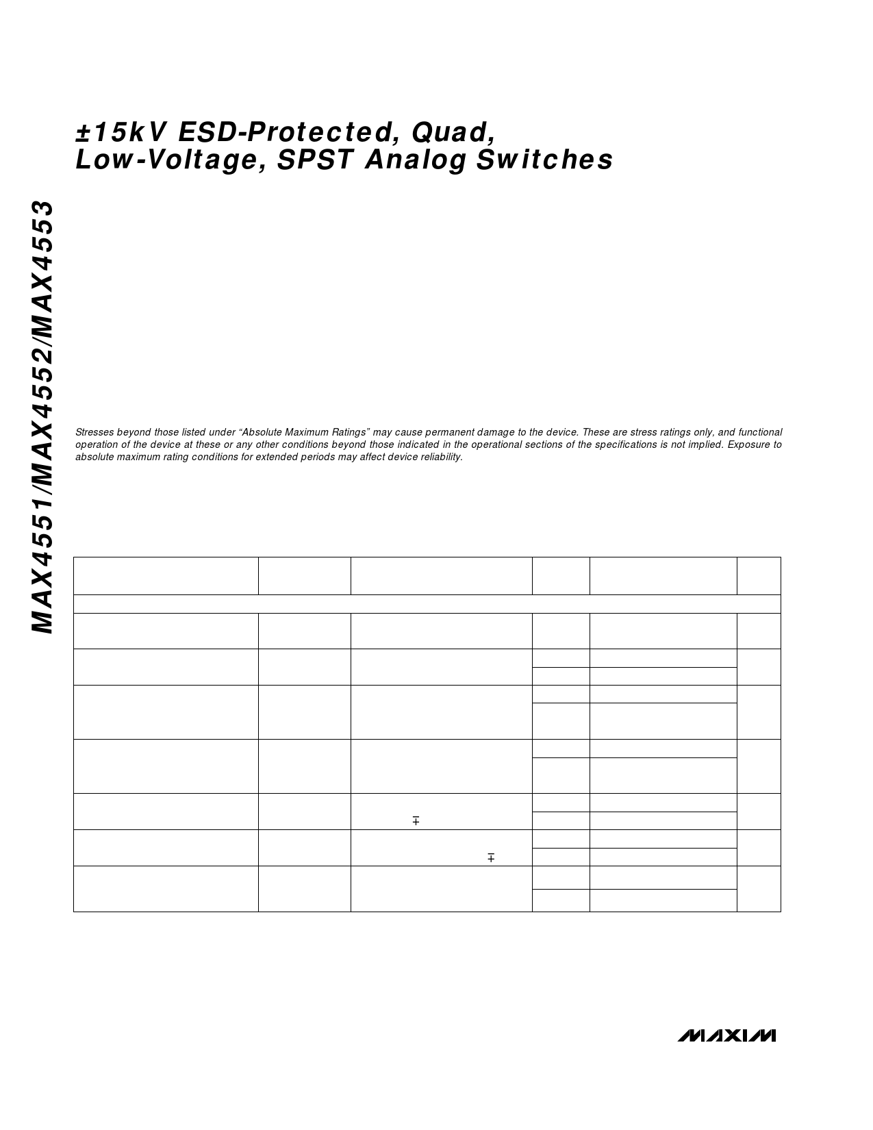
ABSOLUTE MAXIMUM RATINGS
Voltages Referenced to GND
V+.....................................................................-0.3V to +13.0V
V- .....................................................................-13.0V to +0.3V
V+ to V- ............................................................-0.3V to +13.0V
All Other Pins (Note 1) ..........................(V- - 0.3V) to (V+ + 0.3V)
Continuous Current into Any Terminal..............................Вұ10mA
Peak Current into Any Terminal
(pulsed at 1ms,10% duty cycle)...................................Вұ20mA
ESD per Method 3015.7 (IN_, COM_, V+, V-, GND) .......>2500V
IEC 1000-4-2 (NO_, NC_) ..................................................Вұ15kV
Continuous Power Dissipation (TA = +70В°C)
QSOP (derate 9.52mW/В°C above +70В°C) ....................762mW
Narrow SO (derate 8.70mW/В°C above +70В°C) ............696mW
Plastic DIP (derate 10.53mW/В°C above +70В°C) ..........842mW
Operating Temperature Ranges
MAX455_C_E ......................................................0В°C to +70В°C
MAX455_E_E ...................................................-40В°C to +85В°C
Storage Temperature Range .............................-65В°C to +160В°C
Lead Temperature (soldering, 10sec) .............................+300В°C
Note 1: Signals on NC_, NO_, COM_, or IN_ exceeding V+ or V- are clamped by internal diodes. Limit forward-diode current to
maximum current rating.
Stresses beyond those listed under вҖңAbsolute Maximum RatingsвҖқ may cause permanent damage to the device. These are stress ratings only, and functional
operation of the device at these or any other conditions beyond those indicated in the operational sections of the specifications is not implied. Exposure to
absolute maximum rating conditions for extended periods may affect device reliability.
ELECTRICAL CHARACTERISTICSвҖ”Dual Supplies
(V+ = +5V, Вұ10%, V- = -5V, Вұ10%, TA = TMIN to TMAX, unless otherwise noted. Typical values are at TA = +25В°C.)
PARAMETER
ANALOG SWITCH
Analog Signal Range
(Note 3)
COM_ to NO_, COM_ to NC_
On-Resistance
COM_ to NO_, COM_ to NC_
On-Resistance Match Between
Channels (Note 4)
SYMBOL
CONDITIONS
VCOM_, VNO_,
VNC_
RON
V+ = 5V, V- = -5V, VNO_
or VNC_ = Вұ3V, ICOM_ = 1mA
вҲҶRON
V+ = 5V, V- = -5V, VNO_
or VNC_ = Вұ3V, ICOM_ = 1mA
TA
MIN TYP
(Note 2)
C, E
V-
+25В°C
80
C, E
+25В°C
1
C, E
COM_ to NO_, COM_ to NC_
On-Resistance Flatness
(Note 5)
RFLAT(ON)
V+ = 5V, V- = -5V, VNO_
or VNC_ = +3V, 0, -3V
+25В°C
C, E
4
NO_, NC_ Off-Leakage Current
INO_(OFF), V+ = 5.5V, V- = -5.5V,
+25В°C
-1
0.01
(Note 6)
INC_(OFF)
VCOM_ = 4.5V, VNO_ = Вұ4.5V C, E
-10
COM_ Off-Leakage Current
(Note 6)
ICOM_(OFF)
V+ = 5.5V, V- = -5.5V,
VCOM_ = Вұ4.5V, VNO_ = 4.5V
+25В°C
C, E
-1
-10
0.01
COM_ On-Leakage Current
(Note 6)
ICOM_(ON)
V+ = 5.5V, V- = -5.5V,
VCOM_ = Вұ4.5V
+25В°C
-2
0.01
C, E
-20
MAX UNITS
V+ V
120
в„Ұ
140
4
в„Ұ
5
8
в„Ұ
10
1
nA
10
1
nA
10
2
nA
20
2 _______________________________________________________________________________________
Share Link: 