MAX4711CSE データシートの表示(PDF) - Maxim Integrated
部品番号
コンポーネント説明
メーカー
MAX4711CSE Datasheet PDF : 17 Pages
| |||
Fault-Protected, Low-Voltage,
Quad SPST Analog Switches
MAX4711
1, 16, 9, 8
PIN
MAX4712
1, 16, 9, 8
2, 15, 10, 7 2, 15, 10, 7
3, 14, 11, 6
—
—
3, 14, 11, 6
—
—
—
—
4
4
5
5
12
12
13
13
MAX4713
1, 16, 9, 8
2, 15, 10, 7
—
—
3, 6
14, 11
4
5
12
13
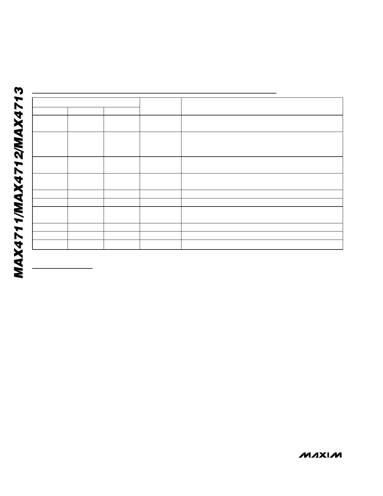
Pin Description
NAME
FUNCTION
IN1, IN2, IN3,
IN4
COM1,
COM2,
COM3, COM4
NC1, NC2,
NC3, NC4
NO1, NO2,
NO3, NO4
NO1, NO4
NC2, NC3
V-
GND
N.C.
V+
Logic Inputs. Fault-protected to (V- + 12V).
Analog Switch Common Terminals
Fault-Protected Analog Switch Normally Closed Terminals
Fault-Protected Analog Switch Normally Open Terminals
Fault-Protected Analog Switch Normally Open Terminals
Fault-Protected Analog Switch Normally Closed Terminals
Negative Supply Voltage Input. Connect to GND for single-supply
operation.
Ground
No Connection. Not internally connected.
Positive Supply Input
Detailed Description
The MAX4711/MAX4712/MAX4713 differ considerably
from traditional fault-protection switches, with several
advantages. First, they are constructed with two paral-
lel FET’s allowing very low on-resistance. Second, they
allow signals on the NC_ or NO_ pins that are within or
slightly beyond the supply rails to be passed through
the switch to the COM terminal, allowing rail-to-rail sig-
nal operation. Third, when a signal on NC_ or NO_
exceeds the supply rails by about 150mV (a fault con-
dition) the voltage on COM_ is limited to the same
polarity supply voltage. Operation is identical for both
fault polarities.
During a fault condition, the NO_ or NC_ input
becomes high impedance regardless of the switch
state or load resistance. If the switch is on, the COM_
output current is supplied from V+ or V- by the clamp
FET’s that are connected from COM to each supply.
These FET’s can typically source or sink up to 15mA.
When power is removed, the fault protection is still in
effect. In this case, the NO_ or NC_ terminals are a vir-
tual open circuit. The fault can be up to ±12V.
The COM_ pins are not fault-protected, they act as nor-
mal CMOS switch terminals. If a voltage source is con-
nected to any COM_ pin, it should be limited to the
supply voltages. Exceeding the supply voltage will
cause high currents to flow through the ESD-protected
diodes, possibly damaging the device (see Absolute
Maximum Ratings).
Pin Compatibility
These switches have identical pinouts to common non-
fault-protected CMOS switches. Care should be exer-
cised while considering them for direct replacements in
existing printed circuit boards since only the NO_ and
NC_ pins of each switch are fault-protected.
Internal Construction
Internal construction is shown in Figure 1, with the ana-
log signal paths shown in bold. A single NO switch is
shown; the NC configuration is identical except the
logic-level translator is inverting. The analog switch is
formed by the parallel combination of N-channel FET
(N1) and P-channel FET (P1), which are driven on and
off simultaneously according to the input fault condition
and the logic-level state.
Normal Operation
Two comparators continuously compare the voltage on
the NO_ (or NC_) pin with V+ and V-. When the signal
on NO_ or NC_ is between V+ and V- the switch acts
normally, with FETs N1 and P1 turning on and off in
response to IN_ signals. The parallel combination of
N1 and P1 forms a low-value resistor between NO_ (or
10 ______________________________________________________________________________________
Share Link: 