MAX4712CSE データシートの表示(PDF) - Maxim Integrated
部品番号
コンポーネント説明
メーカー
MAX4712CSE Datasheet PDF : 17 Pages
| |||
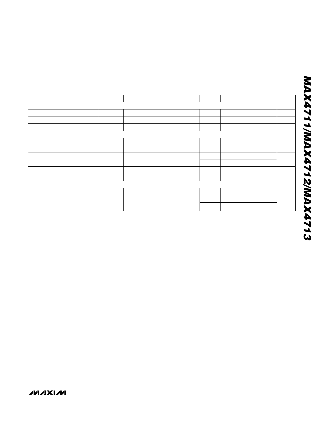
Fault-Protected, Low-Voltage,
Quad SPST Analog Switches
ELECTRICAL CHARACTERISTICS—+3V Single Supply (continued)
(V+ = +2.7V to +3.6V, V- = 0, VIH = +2.0V, VIL = +0.6V, GND = 0, TA = TMIN to TMAX, unless otherwise noted. Typical values are at
TA = +25°C.) (Note 3)
PARAMETER
SYMBOL
CONDITIONS
TA
MIN TYP MAX UNITS
LOGIC INPUT
Input Logic High
VIH
C, E
2
V
Input Logic Low
Input-Leakage Current (Note 5)
SWITCH DYNAMICS
VIL
IIN_
VIN_ = 0 or V+
C, E
C, E
-5
0.6
V
+5
µA
Turn-On Time
Turn-Off Time
tON
V+ = +2.7V, VNO_ or VNC_ = +1.5V,
RL = 300Ω, CL = 35pF, Figure 2
tOFF
V+ = +2.7V, VNO_ or VNC_ = +1.5V,
RL = 300Ω, CL = 35pF, Figure 2
+25°C
C, E
+25°C
C, E
340 500
ns
600
100 175
ns
225
Break-Before-Make Time Delay
(MAX4713 only)
tBBM
V+ = +2.7V, VNO_ or VNC_ = +1.5V,
RL = 300Ω, CL = 35pF, Figure 2
+25°C 60
C, E
50
240
ns
POWER SUPPLY
Power-Supply Range
V+
C, E
2.7
11
V
V+ Supply Current
I+
All VIN_ = 0 or V+
+25°C
C, E
8
15
µA
20
Note 3: Algebraic convention is used in this data sheet; the most negative value is shown in the minimum column.
Note 4: ∆RON = ∆RON(MAX) - ∆RON(MIN)
Note 5: Leakage parameters are 100% tested at maximum-rated temperature and with dual supplies. Leakage parameters are
guaranteed by correlation at +25°C.
Note 6: Off-isolation = 20 log10 [VCOM_/(VNO_ or VNC_)], VCOM_ = output, VNO_ or VNC_ = input to off switch.
Note 7: Between any two switches.
_______________________________________________________________________________________ 7
Share Link: 