MAX496CSE データシートの表示(PDF) - Maxim Integrated
部品番号
コンポーネント説明
メーカー
MAX496CSE Datasheet PDF : 12 Pages
| |||
375MHz Quad Closed-Loop
Video Buffers, AV = +1 and +2
8
6 RL = 50Ω
4 RISO = 0Ω
2
CL = 60pF
CL = 22pF
CL = 47pF
CL = 10pF
0
-2
CL = 0pF
-4
-6
-8
-10
-12
1M
10M
100M
1G
FREQUENCY (Hz)
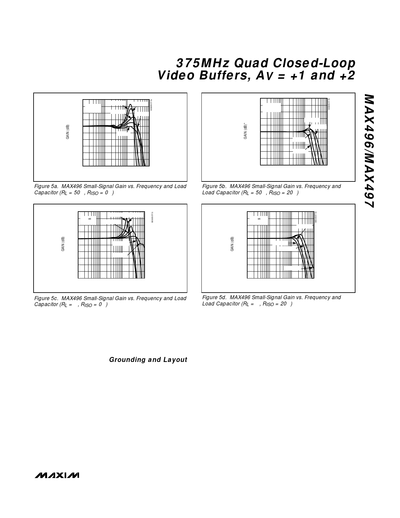
Figure 5a. MAX496 Small-Signal Gain vs. Frequency and Load
Capacitor (RL = 50Ω, RISO = 0Ω)
* -3dB ATTENUATION DUE
TO RISO NOT SHOWN
5
4 RL = 50Ω
3 RISO = 20Ω
2
CL = 22pF
1
CL = 10pF
0
-1
CL = 47pF
-2
-3
CL = 60pF
-4
-5
1M
10M
100M
1G
FREQUENCY (Hz)
Figure 5b. MAX496 Small-Signal Gain vs. Frequency and
Load Capacitor (RL = 50Ω, RISO = 20Ω)
20
15 RL =
10 RISO = 0Ω
CL = 68pF CL = 47pF
CL = 20pF
5
0
-5
CL = 10pF
-10
-15
CL = 0pF
-20
-25
-30
1M
10M
100M
1G
FREQUENCY (Hz)
Figure 5c. MAX496 Small-Signal Gain vs. Frequency and Load
Capacitor (RL = ∞, RISO = 0Ω)
20
15 RL =
10 RISO = 20Ω
5
CL = 47pF
0
-5
CL = 68pF
-10
CL = 22pF
-15
-20
-25
-30
1M
CL = 10pF
10M
100M
1G
FREQUENCY (Hz)
Figure 5d. MAX496 Small-Signal Gain vs. Frequency and
Load Capacitor (RL = ∞, RISO = 20Ω)
The MAX496/MAX497 drive capacitive loads up to 75pF
without sustained oscillation, although some peaking
may occur. When driving larger capacitive loads, or to
reduce peaking, add an isolation resistor (RISO) between
the output and the capacitive load (Figures 5a–5d).
Grounding and Layout
The MAX496/MAX497 bandwidths are in the RF fre-
quency range. Depending on the size of the PC board
used and the frequency of operation, it may be neces-
sary to use Micro-strip or Stripline techniques.
To realize the full AC performance of these high-speed
buffers, pay careful attention to power-supply bypassing
and board layout. The PC board should have at least two
layers (wire-wrap boards are too inductive, bread boards
are too capacitive), with one side a signal layer and the
other a large, low-impedance ground plane. With multilay-
er boards, locate the ground plane on the layer that is not
dedicated to a specific signal trace. The ground plane
should be as free from voids as possible. Connect all
ground pins to the ground plane.
Connect both positive power-supply pins together and
bypass with a 0.10µF ceramic capacitor at each power
supply pin, as close to the device as possible. Repeat
the same for the negative power-supply pins. The
capacitor lead lengths should be as short as possible
to minimize lead inductance; surface-mount chip
capacitors are ideal. A large-value (4.7µF or greater)
tantalum or electrolytic bypass capacitor on each sup-
ply may be required for high-current loads. The location
of this capacitor is not critical.
The MAX496/MAX497’s analog input pins are isolated
with ground pins to minimize parasitic coupling, which can
degrade crosstalk and/or amplifier stability. Keep signal
paths as short as possible to minimize inductance. Ensure
that all input channel traces are the same length to main-
tain the phase relationship between the four channels. To
further reduce crosstalk, connect the coaxial-cable shield
to the ground side of the 75Ω terminating resistor at the
ground plane, and terminate all unused inputs ground and
outputs with a 100Ω or 150Ω resistor to ground.
______________________________________________________________________________________ 11
Share Link: 