MAX519BCSE データシートの表示(PDF) - Maxim Integrated
部品番号
コンポーネント説明
メーカー
MAX519BCSE Datasheet PDF : 16 Pages
| |||
2-Wire Serial 8-Bit DACs with
Rail-to-Rail Outputs
______________________________________________________________Pin Description
MAX517
1
2
—
3
4
—
5
6
7
—
8
—
—
PIN
MAX518
1
2
—
3
4
—
5
6
7
—
—
8
—
MAX519
1
4
5
6
8
9
10
11
12
13
15
16
2, 3, 7, 14
NAME
OUT0
GND
AD3
SCL
SDA
AD2
AD1
AD0
VDD
REF1
REF0
OUT1
N.C.
FUNCTION
DAC0 Voltage Output
Ground
Address Input 3; sets IC’s slave address
Serial Clock Input
Serial Data Input
Address Input 2; sets IC’s slave address
Address Input 1; sets IC’s slave address
Address Input 0; sets IC’s slave address
Power Supply, +5V; used as reference for MAX518
Reference Voltage Input for DAC1
Reference Voltage Input for DAC0
DAC1 Voltage Output
No Connect—not internally connected.
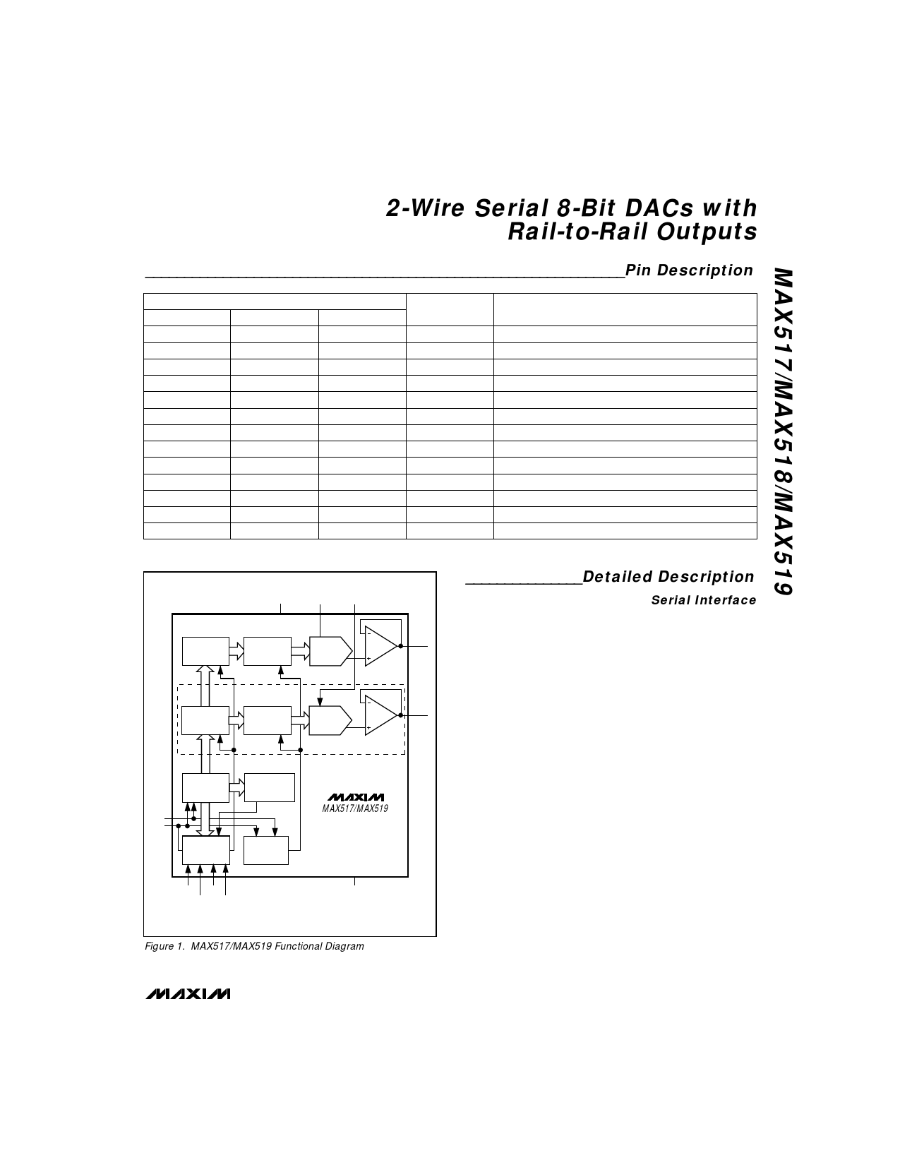
VDD
REF0 (REF1)
INPUT
LATCH 0
OUTPUT
LATCH 0
DAC0
OUT0
INPUT
LATCH 1
OUTPUT
LATCH 1
DAC1
(OUT1)
MAX519 ONLY
8-BIT
SHIFT
REGISTER
ADDRESS
COMPARATOR
SCL
SDA
DECODE
START/STOP
DETECTOR
MAX517/MAX519
AD0 (AD2)
GND
AD1 (AD3)
( ) ARE FOR MAX519
Figure 1. MAX517/MAX519 Functional Diagram
_______________Detailed Description
Serial Interface
The MAX517/MAX518/MAX519 use a simple 2-wire
serial interface requiring only two I/O lines (2-wire bus)
of a standard microprocessor (µP) port. Figure 2 shows
the timing diagram for signals on the 2-wire bus.
Figure 3 shows a typical application. The 2-wire bus can
have several devices (in addition to the MAX517/
MAX518/MAX519) attached. The two bus lines (SDA and
SCL) must be high when the bus is not in use. When in
use, the port bits are toggled to generate the appropriate
signals for SDA and SCL. External pull-up resistors are
not required on these lines. The MAX517/MAX518/
MAX519 can be used in applications where pull-up resis-
tors are required (such as in I2C systems) to maintain
compatibility with existing circuitry.
The MAX517/MAX518/MAX519 are receive-only devices
and must be controlled by a bus master device. They
operate at SCL rates up to 400kHz. A master device
sends information to the devices by transmitting their
address over the bus and then transmitting the desired
information. Each transmission consists of a START
condition, the MAX517/MAX518/MAX519’s programm-
able slave-address, one or more command-byte/out-
put-byte pairs (or a command byte alone, if it is the last
byte in the transmission), and finally, a STOP condition
(Figure 4).
_______________________________________________________________________________________ 7
Share Link: 