MAX5904 データシートの表示(PDF) - Maxim Integrated
部品番号
コンポーネント説明
メーカー
MAX5904 Datasheet PDF : 24 Pages
| |||
Low-Voltage, Dual Hot-Swap Controllers/Power
Sequencers
ABSOLUTE MAXIMUM RATINGS
IN_ to GND...........................................................................+14V
GATE_ to GND..........................................+0.3V to (VIN_ + 6.2V)
ON, PGOOD, COMP+, COMPOUT, TIM
to GND.....-0.3V to the higher of (VIN1 + 0.3V) and (VIN2 + 0.3V)
SENSE_, MON_, LIM_ to GND ...................-0.3V to (VIN_ + 0.3V)
Current into Any Pin .........................................................±50mA
Continuous Power Dissipation (TA = +70°C)
8-Pin Narrow SO (derate 5.9mW/°C above +70°C) ......471mW
16-Pin QSOP (derate 8.3mW/°C above +70°C)............667mW
Operating Temperature Ranges:
MAX590_U_ _ .....................................................0°C to +85°C
MAX590_E_ _ ...................................................-40°C to +85°C
Storage Temperature Range .............................-65°C to +150°C
Lead Temperature (soldering, 10s) .................................+300°C
Stresses beyond those listed under “Absolute Maximum Ratings” may cause permanent damage to the device. These are stress ratings only, and functional
operation of the device at these or any other conditions beyond those indicated in the operational sections of the specifications is not implied. Exposure to
absolute maximum rating conditions for extended periods may affect device reliability.
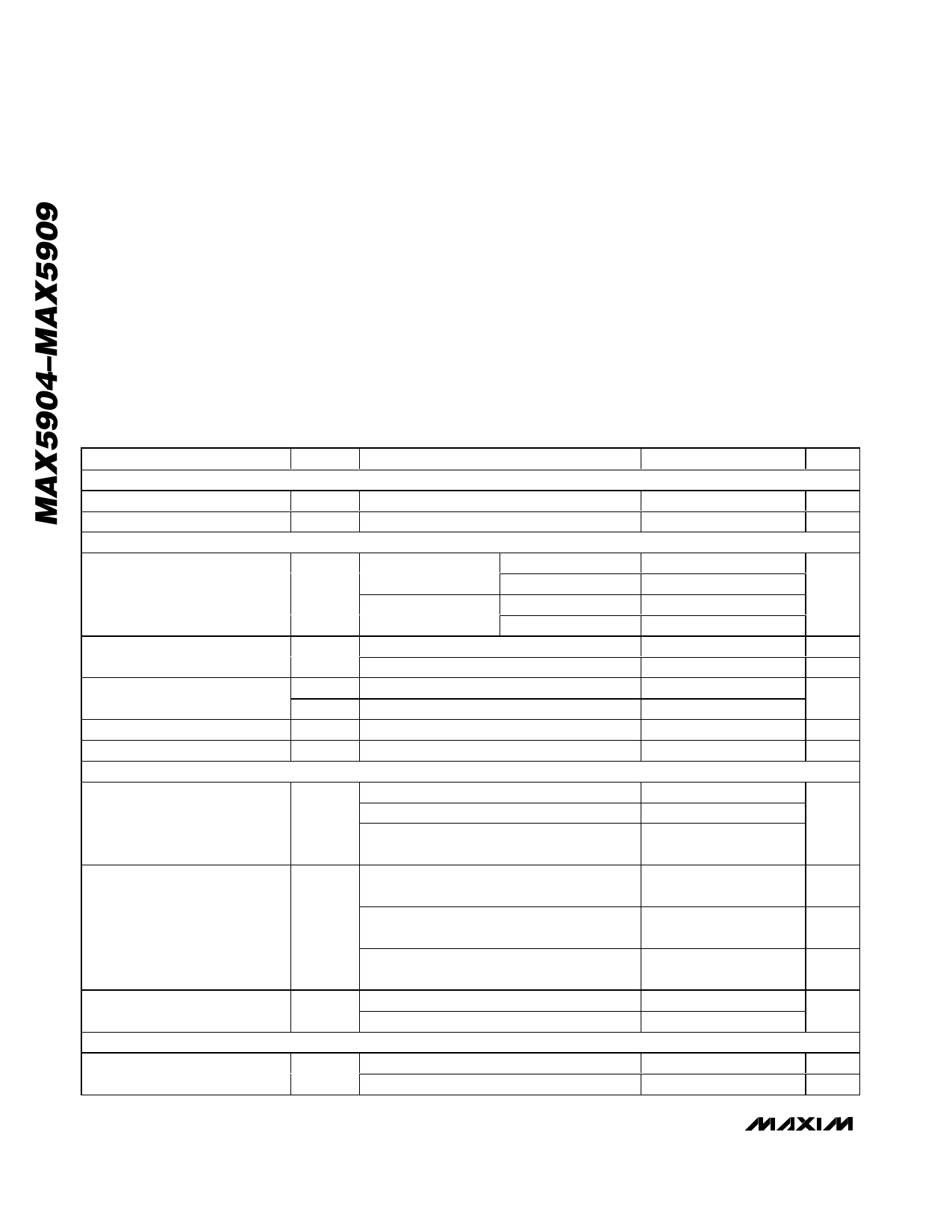
ELECTRICAL CHARACTERISTICS
(VIN_ = +1V to +13.2V provided at least one supply is higher than +2.7V, VON = +2.7V, TA = 0°C to +85°C, unless otherwise noted.
Typical values are at VIN1 = +5V, VIN2 = +3.3V, and TA = +25°C.) (Note 1)
PARAMETER
POWER SUPPLIES
IN_ Input Voltage Range (Note 2)
Supply Current
CURRENT CONTROL
Slow-Comparator Threshold
(VIN - VSENSE) (Note 3)
Slow-Comparator Response Time
(Note 4)
Fast-Comparator Threshold
Fast-Comparator Response Time
SENSE Input Bias Current
MOSFET DRIVER
Startup Period
(Note 5)
SYMBOL
CONDITIONS
VIN_
IIN
Other VIN = +2.7V
IIN1 + IIN2
VSC,TH
tSCD
VSU,TH
VFC,TH
tFCD
IB SEN
MAX5904/MAX5905
TA = +25°C
TA = 0°C to +85°C
LIM = GND
MAX5906–MAX5909
RLIM = 300kΩ
1mV overdrive
50mV overdrive
VIN_ - VSENSE_; during startup
VIN_ - VSENSE_; normal operation
10mV overdrive, from overload condition
VSEN_ = VIN_
tSTART
RTIM = 100kΩ
RTIM = 4kΩ (minimum value)
TIM floating for MAX5906–MAX5909
fixed for MAX5904/MAX5905
MIN TYP MAX UNITS
1.0
1.2
13.2
V
2.9
mA
22.5 25
27.5
20.5
27.5
mV
22.5
25
27.5
80
100 125
3
ms
110
µs
2 x VSC, TH
mV
4 x VSC, TH
260
ns
0.03
6
µA
7.1 10.8 15.5
0.31 0.45 0.58
ms
3.9
9
16.0
Charging, VGATE = +5V, VIN = +10V
(Note 5)
80
100
130
µA
Average Gate Current
IGATE
Weak discharge, during startup when current
limit is active or when 0.4V < VON < 0.8V
100
µA
Gate-Drive Voltage
ON COMPARATOR
Fast Pulldown ON Threshold
VDRIVE
Strong discharge, triggered by a fault or
when VON < 0.4V
VGATE_ - VIN_, IGATE_ < 1µA, VIN ≥ 3V
VGATE_ - VIN_, IGATE_ < 1µA, 2.7V ≤ VIN ≤ 3V
3
4.8 5.4
4.2 5.3
Low to high
VONFP,TH Hysteresis
0.375 0.4
25
mA
5.8
V
5.8
0.425
V
mV
2 _______________________________________________________________________________________
Share Link: 