MAX5941BCSE データシートの表示(PDF) - Maxim Integrated
部品番号
コンポーネント説明
メーカー
MAX5941BCSE
Maxim Integrated

MAX5941BCSE Datasheet PDF : 24 Pages
| |||
IEEE 802.3af-Compliant Power-Over-Ethernet
Interface/PWM Controller for Power Devices
ABSOLUTE MAXIMUM RATINGS
(All voltages are referenced to VEE, unless otherwise noted.)
GND........................................................................-0.3V to +90V
OUT, PGOOD ...........................................-0.3V to (GND + 0.3V)
RCL, GATE .............................................................-0.3V to +12V
UVLO ........................................................................-0.3V to +8V
PGOOD to OUT.........................................-0.3V to (GND + 0.3V)
V+ to V-...................................................................-0.3V to +90V
VDD to V-.................................................................-0.3V to +40V
VCC to V-..............................................................-0.3V to +12.5V
OPTO, NDRV, SS_SHDN, CS to V-.............-0.3V to (VCC + 0.3V)
Maximum Input/Output Current (Continuous)
OUT to VEE ...................................................................500mA
GND, RCL to VEE ............................................................70mA
UVLO, PGOOD, PGOOD to VEE .....................................20mA
GATE to VEE....................................................................80mA
VDD, VCC.........................................................................20mA
NDRV Continuous ...........................................................25mA
NDRV (Pulsed for less than 1µs) .......................................±1A
Continuous Power Dissipation (TA = +70°C)
16-Pin SO (derate 9.1mW/°C above +70°C)................727mW
Operating Temperature Range
MAX5941_CSE ..................................................0°C to +70°C
MAX5941_ESE ...............................................-40°C to +85°C
Storage Temperature Range .............................-65°C to +150°C
Junction Temperature ......................................................+150°C
Lead Temperature (soldering, 10s) ................................+300°C
Stresses beyond those listed under “Absolute Maximum Ratings” may cause permanent damage to the device. These are stress ratings only, and functional
operation of the device at these or any other conditions beyond those indicated in the operational sections of the specifications is not implied. Exposure to
absolute maximum rating conditions for extended periods may affect device reliability.
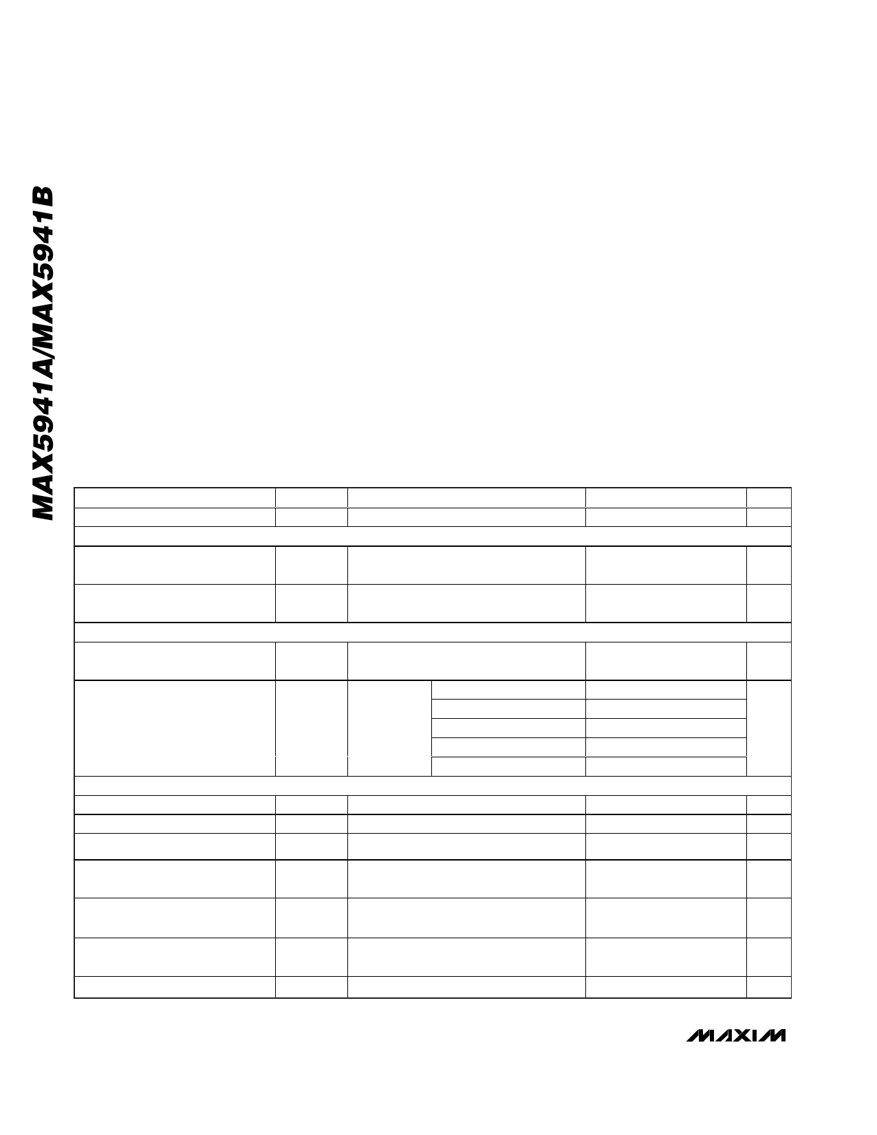
ELECTRICAL CHARACTERISTICS
(VIN = (GND - VEE) = 48V, GATE = PGOOD = PGOOD = OPEN, V- tied to OUT, V+ tied to GND, UVLO = VEE, TA = TMIN to +TMAX,
unless otherwise noted. Typical values are at TA = +25°C. All voltages are referenced to VEE, unless otherwise noted.) (Note 1)
PARAMETER
PD INTERFACE
DETECTION MODE
SYMBOL
CONDITIONS
MIN
TYP MAX UNITS
Input Offset Current
IOFFSET
VIN = 1.4V to 10.1V, GND = V- = OUT = V+
(Note 2)
10
µA
Effective Differential Input
Resistance
dR
VIN = 1.4V up to 10.1V with 1V step, OUT =
PGOOD = GND = OUT = V+ (Note 3)
550
kΩ
CLASSIFICATION MODE
Classification Current Turn-Off
Threshold
Classification Current (Notes 5, 6)
POWER MODE
Operating Supply Voltage
Operating Supply Current
VTH,CLSS VIN rising (Note 4)
ICLASS
VIN = 12.6V
to 20V, RDISC
= 25.5kΩ
Class 0, RCL = 10kΩ
Class 1, RCL = 732Ω
Class 2, RCL = 392Ω
Class 3, RCL = 255Ω
Class 4, RCL = 178Ω
VIN
VIN = (GND - VEE)
IIN
Measure at GND, not including RDISC
20.8 21.8 22.5
V
0
9.17
17.29
26.45
36.6
2
11.83
19.71 mA
29.55
41.4
67
V
0.4
1
mA
Default Power Turn-On Voltage
VUVLO, ON VIN increasing, UVLO = VEE
37.4 38.6 40.1
V
Default Power Turn-Off Voltage
VUVLO, OFF VIN decreasing, UVLO = VEE
30
V
Default Power Turn-On/Off
Hysteresis
External UVLO Programming
Range
UVLO External Reference Voltage
VHYST,
UVLO
VIN,EX Set UVLO externally (Note 7)
VREF, UVLO VUVLO increasing
7.4
V
12
67
V
2.400 2.460 2.522
V
2 _______________________________________________________________________________________
Share Link: