MAX5941BCSE データシートの表示(PDF) - Maxim Integrated
部品番号
コンポーネント説明
メーカー
MAX5941BCSE
Maxim Integrated

MAX5941BCSE Datasheet PDF : 24 Pages
| |||
IEEE 802.3af-Compliant Power-Over-Ethernet
Interface/PWM Controller for Power Devices
Note 1: All min/max limits for the PD interface are production tested at +85°C (extended grade)/+70°C (commercial grade). Limits
at +25°C and -40°C are guaranteed by design. All PWM controller min/max limits are 100% production tested at +25°C
and +85°C (extended grade)/+70°C (commercial grade). Limits at -40°C are guaranteed by design, unless otherwise
noted.
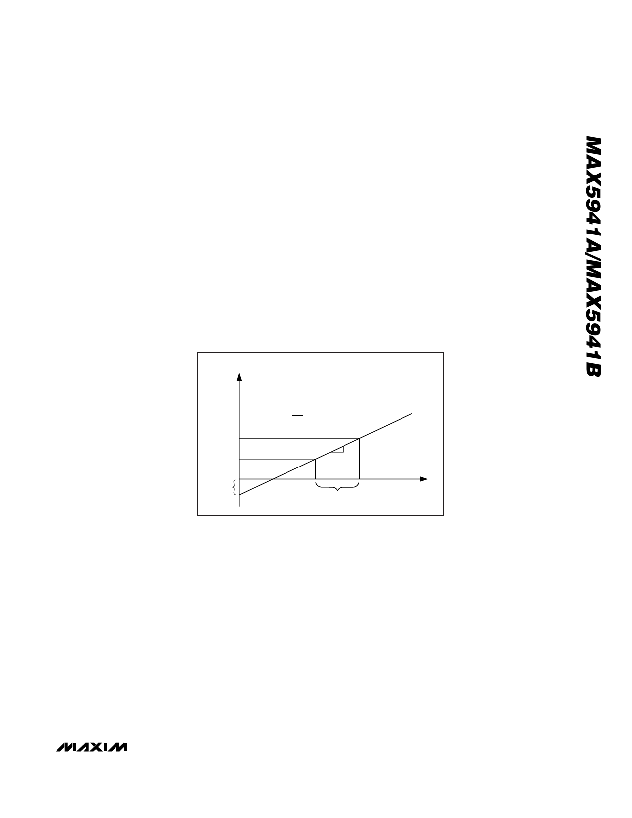
Note 2: The input offset current is illustrated in Figure 1.
Note 3: Effective differential input resistance is defined as the differential resistance between GND and VEE without any external
resistance.
Note 4: Classification current is turned off whenever the IC is in power mode.
Note 5: See Table 2 in the PD Classification Mode section. RDISC and RCL must be 100ppm or better.
Note 6: See Thermal Dissipation section for details.
Note 7: When UVLO is connected to the midpoint of an external resistor-divider with a series resistance of 25.5kΩ (±1%), the turn-
on threshold set point for the power mode is defined by the external resistor-divider. Make sure the voltage on the UVLO
pin does not exceed its maximum rating of 8V when VIN is at the maximum voltage.
Note 8: When the VUVLO is below VTH, G, UVLO, the MAX5941 sets the turn-on voltage threshold internally (VUVLO,ON).
Note 9: An input voltage or VUVLO glitch below their respective thresholds shorter than or equal to tOFF_DLY does not cause the
MAX5941A/MAX5941B to exit power-on mode (as long as the input voltage remains above an operable voltage level of 12V).
Note 10: PGOOD references to OUT while PGOOD references to VEE.
Note 11: Guaranteed by design.
IIN
IINi +1
IINi
dRi
≅
(VINi
(IINi
+
+
1
1
-
-
VINi)
IINi)
=
(IINi
1V
+1
-
IINi)
IOFFSET
≅
IINi
-
VINi
dRi
dRi
IOFFSET
VINi 1V VINi +1
Figure 1. Effective Differential Input Resistance/Offset Current
_______________________________________________________________________________________ 5
Share Link: