MAX8790A データシートの表示(PDF) - Maxim Integrated
部品番号
コンポーネント説明
メーカー
MAX8790A
Maxim Integrated

MAX8790A Datasheet PDF : 22 Pages
| |||
MAX8790A
Six-String White LED Driver with Active
Current Balancing for LCD Panel Applications
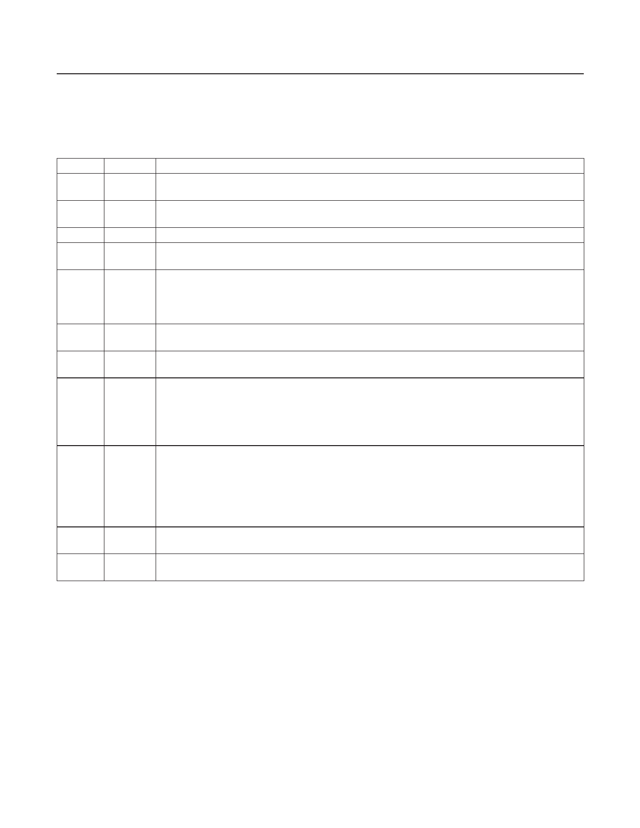
Pin Description (continued)
PIN
NAME
FUNCTION
11
FB6
LED String 6 Cathode Connection. FB6 is the open-drain output of an internal regulator, which controls
current through FB6. FB6 can sink up to 27mA. If unused, connect FB6 to GND.
12
CS
Step-Up Controller Current-Sense Input. Connect the CS input to a ground-referenced sense resistor to
measure the current in the external MOSFET switch.
13
EXT External MOSFET Gate-Drive Output
14
OV
Overvoltage Sense. Connect OV to the center tap of a resistive voltage-divider from VOUT to ground. The
detection threshold for voltage limiting at OV is 1.23V (typ).
5V Linear Regulator Output. VCC provides power to the MAX8790A and is also used to bias the gate driver
15
VCC
for the external MOSFET. Bypass VCC to GND with a ceramic capacitor of 1µF or greater. If VIN is less
than or equal to 5.5V, connect VCC to IN to the disable the internal LDO and use the external 5V supply to
VCC. When SHDN is low, the internal linear regulator is disabled.
16
IN
Supply Input. VIN biases the internal 5V linear regulator that powers the device. Bypass IN to GND directly
at the pin with a 0.1µF or greater ceramic capacitor.
17
CCV
Step-Up Converter Compensation Pin. Connect a 0.1µF ceramic capacitor and 1.2kΩ resistor from CCV to
GND. When the MAX8790A shuts down, CCV is discharged to 0V through an internal 20kΩ resistor.
Full-Scale LED Current Adjustment Pin. The resistance from ISET to GND controls the full-scale current in
each LED string:
18
ISET
ILEDmax = 20mA x 100kΩ/RISET
The acceptable resistance range is 74kΩ < RISET < 133kΩ, which corresponds to full-scale LED current of
27mA > ILEDmax > 15mA. Connect ISET to VCC for a default full-scale LED current of 20mA.
PLL Free-Running Frequency Control Pin. The resistance from FSET to GND controls the PLL oscillator’s
free-running frequency, fPLL:
19
FSET
fPLL = 1 / (10 x RFSET x 800pF)
The capture range is 0.6 x fPLL to fPLL. The acceptable resistance range for FSET is 250kΩ < RFSET <
754kΩ, which corresponds to a frequency range of 500Hz > fPLL > 166Hz. The resulting capture frequency
range is 100Hz to 500Hz.
20
CPLL
Phase-Locked Loop-Compensation Capacitor Pin. The capacitance at CPLL compensates the PLL loop
response. Connect a 0.1µF ceramic capacitor from CPLL to GND.
EP
EP
Exposed Backside Pad. Solder to the circuit board ground plane with sufficient copper connection to
ensure low thermal resistance. See the PCB Layout Guidelines section.
www.maximintegrated.com
Maxim Integrated │ 9
Share Link: