MAX901ACSE データシートの表示(PDF) - Maxim Integrated
部品番号
コンポーネント説明
メーカー
MAX901ACSE Datasheet PDF : 12 Pages
| |||
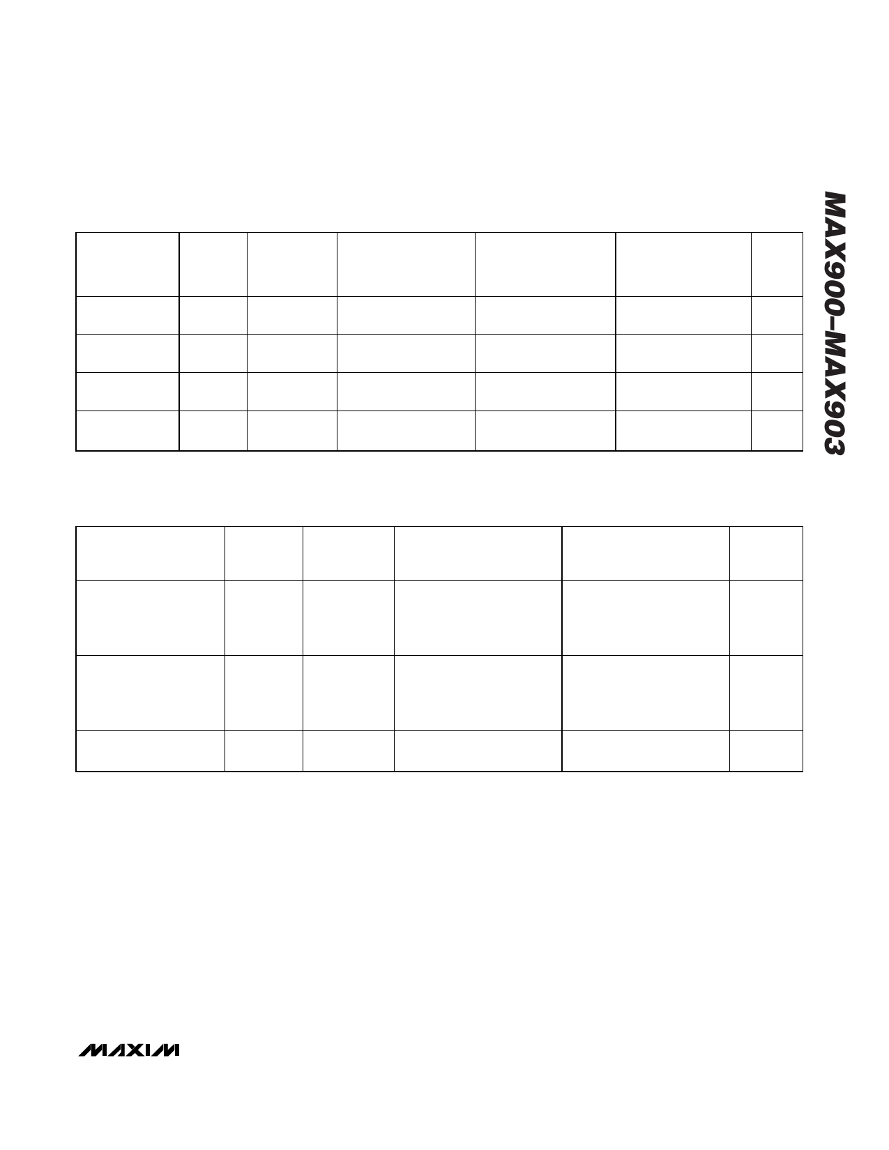
High-Speed, Low-Power Voltage Comparators
ELECTRICAL CHARACTERISTICS (continued)
(VCC = +5V, VEE = -5V, VDD = +5V, LE1–LE4 = logic high, TA = full operating temperature, unless otherwise noted.)
PARAMETER
Positive Analog
Supply Current
Negative Analog
Supply Current
Digital Supply
Current
Power
Dissipation
SYMBOL CONDITIONS
ICC
(Note 7)
IEE
(Note 7)
IDD
(Note 7)
PD
VCC = VDD =
+5V, VEE = 0
MAX900A/MAX901A/
MAX900B/MAX901B
MIN TYP MAX
10 25
7
20
4
10
70 105
MAX902
MAX903
MIN TYP MAX MIN TYP MAX
5
12
2.5
6
3.5 10
2
5
2
5
1
2.5
35
55
18
28
UNITS
mA
mA
mA
mW
TIMING CHARACTERISTICS
(VCC = +5V, VEE = -5V, VDD = +5V, LE1–LE4 = logic high, TA = full operating temperature, unless otherwise noted.)
PARAMETER
Input-to-Output High
Response Time
SYMBOL CONDITIONS
VOD = 5mV,
tpd+
CL = 15pF,
IO = 2mA
(Note 4)
MAX900A/MAX901A
MIN
TYP
MAX
10
15
MAX900B/MAX901B/
MAX902/MAX903
MIN
TYP
MAX
10
15
UNITS
ns
Input-to-Output Low
Response Time
Difference in Response
Time Between Outputs
tpd-
∆tpd
VOD = 5mV,
CL = 15pF,
IO = 2mA
(Note 4)
(Notes 4, 5)
10
15
1
3
10
15
ns
1
3
ns
Note 1: The input common-mode voltage and input signal voltages should not be allowed to go negative by more than 0.2V below
VEE. The upper-end of the common-mode voltage range is typically VCC - 2V, but either or both inputs can go to a maximum
of VCC + 0.2V without damage.
Note 2: Tested for +4.75V < VCC < +5.25V, and -5.25V < VEE < -4.75V with VDD = +5V, although permissible analog power-supply
range is +4.75V < VCC < +10.5V for single-supply operation with VEE grounded.
Note 3: Specification does not apply to MAX901.
Note 4: Guaranteed by design. Times are for 100mV step inputs (see Propagation Delay Characteristics in Figures 2 and 3).
Note 5: Maximum difference in propagation delay between any of the four comparators in the MAX900–MAX903.
Note 6: See Timing Diagram (Figure 2). Owing to the difficult and critical nature of switching measurements involving the latch,
these parameters cannot be tested in a production environment. Typical specifications listed are taken from measurements
using a high-speed test-jig.
Note 7: ICC tested for +4.75V < VCC < +10.5V with VEE grounded. IEE tested for -5.25V < VEE < -4.75V with VCC = +5V. IDD tested
for +4.75V < VDD < +5.25V with the worst-case condition of all four comparator outputs at logic low.
_______________________________________________________________________________________ 5
Share Link: 