MAX913CSA(2003) データシートの表示(PDF) - Maxim Integrated
部品番号
コンポーネント説明
メーカー
MAX913CSA Datasheet PDF : 11 Pages
| |||
Single/Dual, Ultra-Fast, Low-Power
Precision TTL Comparators
Applications Information
Power Supplies and Bypassing
The MAX912/MAX913 are tested with ±5V power sup-
plies that provide an input common-mode range (VCM)
of 8.7V (-5.2V to +3.5V). Operation from a single +5V
supply provides a common-mode input range of 3.7V
(-0.2V to +3.5). Connect V- to GND for single-supply
operation. The MAX912/MAX913 will operate from a
minimum single-supply voltage of +4.5V.
The V+ supply provides power to both the analog input
stage and digital output circuits, whereas the V- supply
only powers the analog section. Bypass V+ and V- to
ground with 0.1µF to 1.0µF ceramic capacitors in parallel
with 10µF or greater tantalum capacitors. Connect the
ceramic capacitors very close to the MAX912/MAX913’s
supply pins, keeping leads short to minimize lead induc-
tance. For particularly noisy applications, use ferrite
beads on the power-supply lines.
Board Layout
As with all high-speed components, careful attention to
layout is essential for best performance.
1) Use a printed circuit board with an unbroken ground
plane.
2) Pay close attention to the bandwidth of bypass com-
ponents and keep leads short.
3) Avoid sockets; solder the comparator and other
components directly to the board to minimize
unwanted parasitic inductance and capacitance.
Input Slew Rate
The MAX912/MAX913 design eliminates the input slew-
rate requirement imposed on many standard compara-
tors. As long as LE is high after the maximum propaga-
tion delay and the input is greater than the
comparator’s total DC error, the output will be valid
without oscillations.
Maximum Clock (LE) and Signal Rate
The maximum clock and signal rate is 70MHz, based
on the comparator’s rise and fall time with a 5mV over-
drive at +25°C (Figure 1). With a 20mV overdrive, the
maximum propagation delay is 12ns and the clock sig-
nal rate is 85MHz.
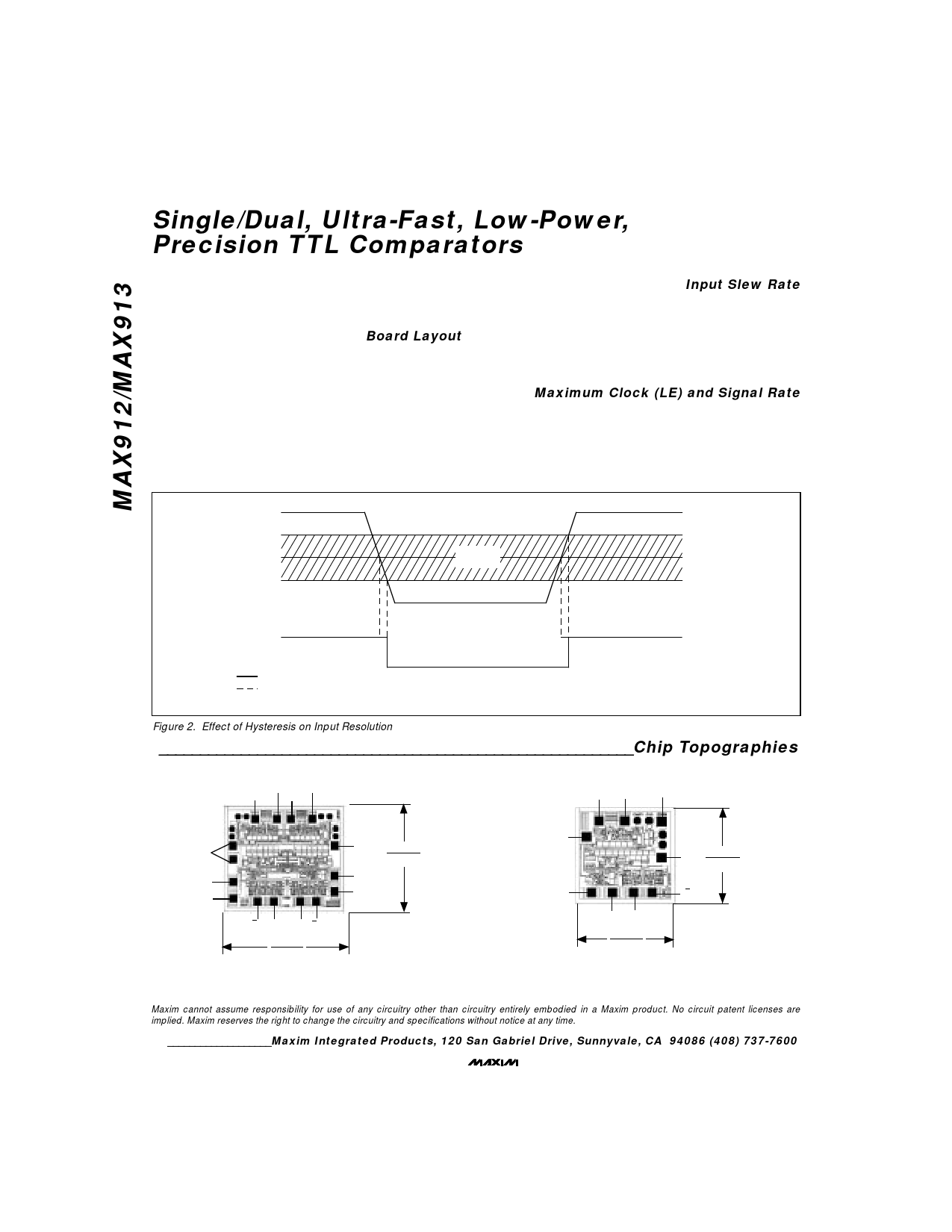
IN+
IN-
HYSTERESIS
BAND*
Q
WITH HYSTERESIS
IDEAL (WITHOUT HYSTERESIS)
*WHEN HYSTERESIS IS ADDED, A COMPARATOR CANNOT RESOLVE ANY INPUT SIGNAL WITHIN THE HYSTERESIS BAND.
Figure 2. Effect of Hysteresis on Input Resolution
Chip Information
MAX912 TRANSISTOR COUNT: 285
MAX913 TRANSISTOR COUNT: 154
PROCESS: Bipolar
8 _______________________________________________________________________________________
Share Link: 