MB3845PFV-ER データシートの表示(PDF) - Fujitsu
部品番号
コンポーネント説明
メーカー
MB3845PFV-ER Datasheet PDF : 19 Pages
| |||
MB3842/MB3845
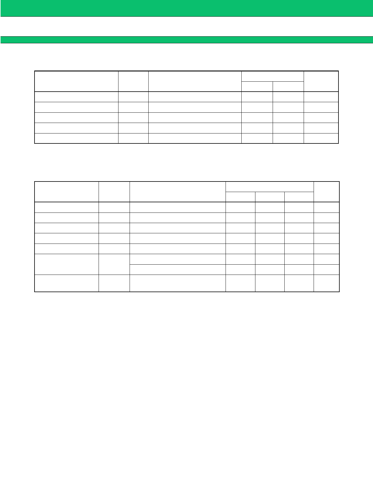
s ABSOLUTE MAXIMUM RATINGS
Parameter
Input voltage
ENABLE voltage
Switch current
Power dissipation
Storage temperature
Symbol
Condition
VIN
VEN
ISW
PD
TSTG
—
—
—
Ta = +85°C
—
Rating
Unit
Max.
Min.
–0.3
7.0
V
–0.3
7.0
V
—
1.8
A
—
216
mW
–55
+125
°C
WARNING: Semiconductor devices can be permanently damaged by application of stress (voltage, current,
temperature, etc.) in excess of absolute maximum ratings. Do not exceed these ratings.
s RECOMMENDED OPERATING CONDITIONS
Parameter
Symbol
Condition
Min.
Value
Typ.
Max.
Input voltage
ENABLE voltage
VIN
—
VEN
VEN ≤ VIN
2.5
5.0
5.5
0
—
5.5
Switch current
ISW
VIN = 2.5 V to 5.5 V
—
—
0.6
SS pin capacitance
CSS*
—
—
—
10
OC sink current
IOCS
VIN = 5.0 V, VOC = 0.4 V
2.0
5.0
—
Current limit
resistance
RLIM*
VIN = 5.0 V (ISW = 0.6 A)
VIN = 5.0 V (ISW = 0.1 A)
1.4
2.0
2.6
3.6
6.2
9.1
Operating
temperature
TOP
—
–20
—
+85
* : For CSS, RLIM settings, see “TYPICAL CHARACTERISTICS” and “FUNCTIONAL DESCRIPTION”.
Unit
V
V
A
nF
mA
kΩ
kΩ
°C
WARNING: The recommended operating conditions are required in order to ensure the normal operation of the
semiconductor device. All of the device's electrical characteristics are warranted when the device is
operated within these ranges.
Always use semiconductor devices within their recommended operating condition ranges. Operation
outside these ranges may adversely affect reliability and could result in device failure.
No warranty is made with respect to uses, operating conditions, or combinations not represented on
the data sheet. Users considering application outside the listed conditions are advised to contact their
FUJITSU representatives beforehand.
5
Share Link: 