MB90F483C データシートの表示(PDF) - Fujitsu
部品番号
コンポーネント説明
メーカー
MB90F483C Datasheet PDF : 124 Pages
| |||
MB90480B/485B Series
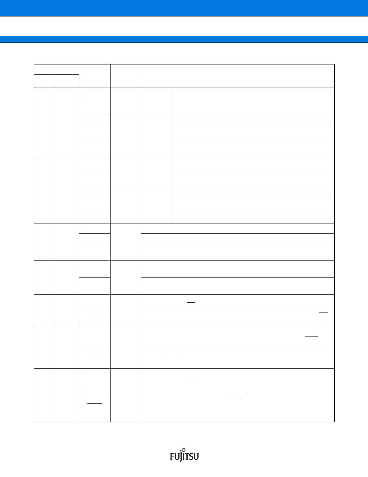
Pin No.
Pin name
QFP*1 LQFP*2
I/O
circuit
type*3
Function
P43, P44
This is a general purpose I/O port.
A11, A12
F (CMOS)
MB90480B
series
In non-multiplex mode, these pins function as external
address pins.
21, 22 19, 20
P43, P44
This is a general purpose I/O port.
A11, A12
MT00,
MT01
F (CMOS)
MB90485B
series
In non-multiplex mode, these pins function as external
address pins.
PG output pins
P45
This is a general purpose I/O port.
F
MB90480B
A13
(CMOS) series In non-multiplex mode, this pin functions as an external
address pin.
24
22
P45
This is a general purpose I/O port.
A13
G
MB90485B In non-multiplex mode, this pin functions as an external
(CMOS/H) series address pin.
EXTC*4
PG input pin.
P46, P47
This is a general purpose I/O port.
25, 26 23, 24
A14, A15
OUT4,
OUT5
F In non-multiplex mode, these pins function as external address pins.
(CMOS)
Output compare event output pins.
70
68
P50
This is a general purpose I/O port. In external bus mode, this pin
D
functions as the ALE pin.
ALE
(CMOS) In external bus mode, this pin functions as the address load enable
(ALE) signal pin.
71
69
P51
This is a general purpose I/O port. In external bus mode, this pin
D
functions as the RD pin.
RD
(CMOS) In external bus mode, this pin functions as the read strobe output (RD)
signal pin.
72
70
P52
WRL
D
(CMOS)
This is a general purpose I/O port. In external bus mode, when the WRE
bit in the EPCR register is set to “1”, this pin functions as the WRL pin.
In external bus mode, this pin functions as the lower data write strobe
output (WRL) pin. When the WRE bit in the EPCR register is set to “0”,
this pin functions as a general purpose I/O port.
73
71
P53
WRH
D
(CMOS)
This is a general purpose I/O port. In external bus mode with 16-bit bus
width, when the WRE bit in the EPCR register is set to “1”, this pin
functions as the WRH pin.
In external bus mode with 16-bit bus width, this pin functions as the
upper data write strobe output (WRH) pin. When the WRE bit in the
EPCR register is set to “0”, this pin functions as a general purpose I/O
port.
(Continued)
10
DS07-13722-11E
Share Link: 