MBRB20200CT データシートの表示(PDF) - ON Semiconductor
部品番号
コンポーネント説明
メーカー
MBRB20200CT Datasheet PDF : 5 Pages
| |||
MBRB20200CT
SWITCHMODEt
Power Rectifier
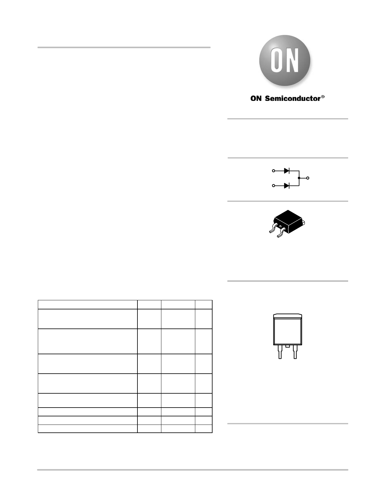
Dual Schottky Rectifier
This device uses the Schottky Barrier technology with a platinum
barrier metal. This state−of−the−art device is designed for use in high
frequency switching power supplies and converters with up to 48 V
outputs. They block up to 200 V and offer improved Schottky
performance at frequencies from 250 kHz to 5.0 MHz.
Features
• 200 V Blocking Voltage
• Low Forward Voltage Drop
• Guardring for Stress Protection and High dv/dt Capability
(10,000 V/ms)
• Dual Diode Construction − Terminals 1 and 3 Must be Connected for
Parallel Operation at Full Rating
• Pb−Free Packages are Available
http://onsemi.com
SCHOTTKY BARRIER
RECTIFIER
20 AMPERES, 200 V
1
4
3
Mechanical Characteristics:
• Case: Epoxy, Molded, Epoxy Meets UL 94 V−0
• Weight: 1.7 Grams (Approximately)
• Finish: All External Surfaces Corrosion Resistant and Terminal
Leads are Readily Solderable
• Lead and Mounting Surface Temperature for Soldering
Purposes: 260°C Max. for 10 Seconds
• Device Meets MSL1 Requirements
MAXIMUM RATINGS (Per Leg)
Rating
Symbol
Value
Unit
Peak Repetitive Reverse Voltage
Working Peak Reverse Voltage
DC Blocking Voltage
VRRM
200
V
VRWM
VR
Average Rectified Forward Current
IF(AV)
A
(At Rated VR, TC = 134°C)
Per Leg
10
Per Device
20
Peak Repetitive Forward Current
IFRM
20
A
(At Rated VR, Square Wave, 20 kHz,
TC = +137°C) Per Leg
Nonrepetitive Peak Surge Current
IFSM
150
A
(Surge Applied at Rated Load Conditions
Halfwave, Single Phase, 60 Hz)
Peak Repetitive Reverse Surge Current
IRRM
1.0
A
(2.0 ms, 1.0 kHz)
Storage Temperature Range
Tstg −65 to +175 °C
Operating Junction Temperature
TJ
−65 to +150 °C
Voltage Rate of Change (Rated VR)
dv/dt
10,000 V/ms
Maximum ratings are those values beyond which device damage can occur.
Maximum ratings applied to the device are individual stress limit values (not
normal operating conditions) and are not valid simultaneously. If these limits are
exceeded, device functional operation is not implied, damage may occur and
reliability may be affected.
4
1
3
D2PAK
CASE 418B
PLASTIC
MARKING DIAGRAM
AY WW
B20200G
AKA
A
Y
WW
B20200
G
AKA
= Assembly Location
= Year
= Work Week
= Device Code
= Pb−Free Package
= Diode Polarity
ORDERING INFORMATION
See detailed ordering and shipping information in the package
dimensions section on page 2 of this data sheet.
© Semiconductor Components Industries, LLC, 2005
1
September, 2005 − Rev. 6
Publication Order Number:
MBRB20200CT/D
Share Link: 