MC100ELT28D(2008) データシートの表示(PDF) - ON Semiconductor
部品番号
コンポーネント説明
メーカー
MC100ELT28D
(Rev.:2008)
(Rev.:2008)
ON Semiconductor

MC100ELT28D Datasheet PDF : 9 Pages
| |||
MC10ELT28, MC100ELT28
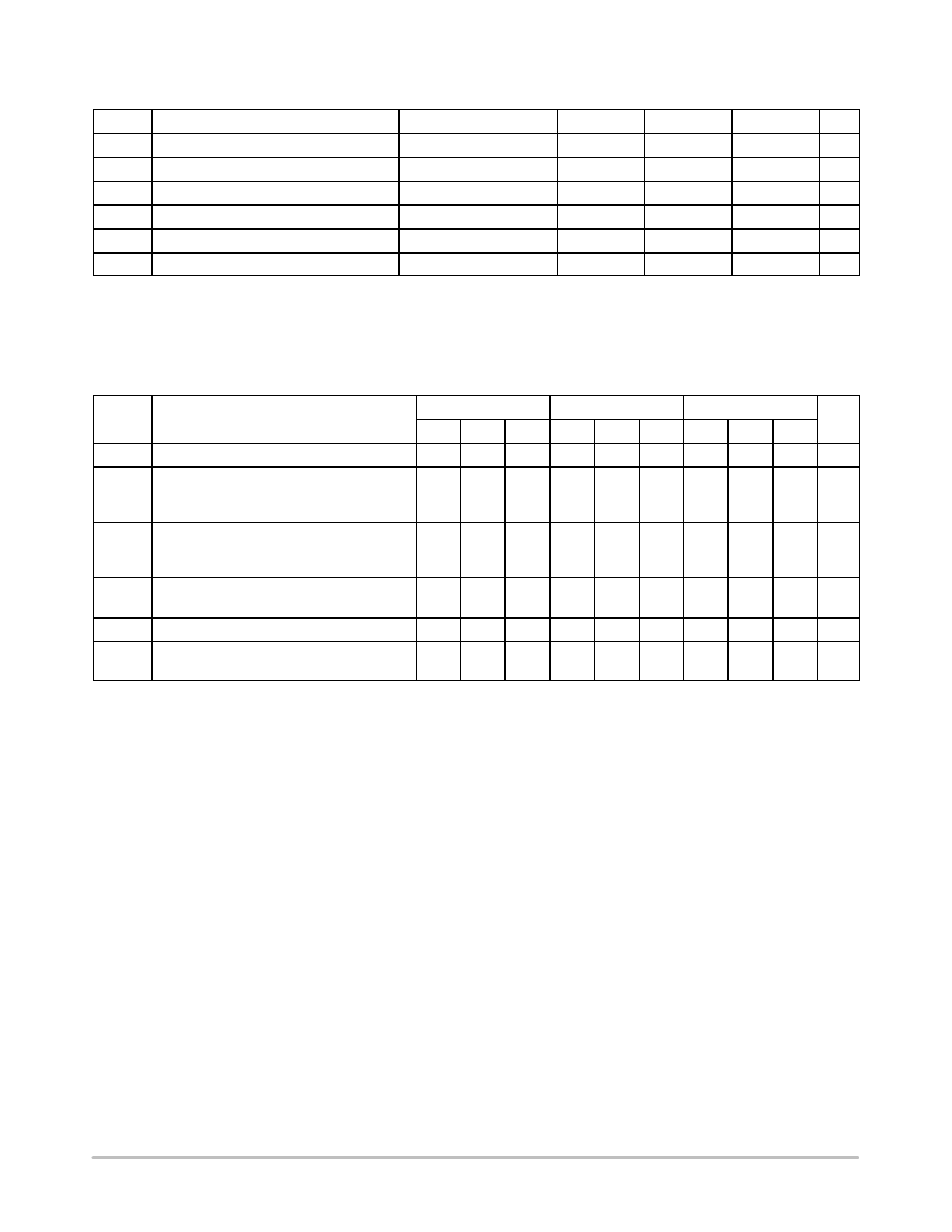
Table 7. TTL INPUT DC CHARACTERISTICS VCC = 4.75 V to 5.25 V; TA = −40°C to 85°C
Symbol
Characteristic
Condition
Min
Typ
Max
Unit
IIH
Input HIGH Current
IIHH
Input HIGH Current
IIL
Input LOW Current
VIK
Input Clamp Diode Voltage
VIN = 2.7 V
VIN = 7.0 V
VIN = 0.5 V
IIN = −18 mA
20
mA
100
mA
−0.6
mA
−1.2
V
VIH
Input HIGH Voltage
2.0
V
VIL
Input LOW Voltage
0.8
V
NOTE: Device will meet the specifications after thermal equilibrium has been established when mounted in a test socket or printed circuit
board with maintained transverse airflow greater than 500 lfpm. Electrical parameters are guaranteed only over the declared
operating temperature range. Functional operation of the device exceeding these conditions is not implied. Device specification
limit values are applied individually under normal operating conditions and not valid simultaneously.
Table 8. AC CHARACTERISTICS VCC = 4.75 V to 5.25 V (Note 9)
−40°C
25°C
85°C
Symbol
Characteristic
Min Typ Max Min Typ Max Min Typ Max Unit
fmax
Maximum Toggle Frequency
TBD
100
TBD
MHz
tPLH
Propagation Delay @ 1.5 V
DECL to QTTL 2.0
DTTL to QECL 0.6
5.5 2.0
5.5 2.0
1.2 0.9 1.2 1.5 0.6
ns
5.5
1.35
tPHL
Propagation Delay @ 1.5 V
DECL to QTTL 2.0
DTTL to QECL 0.4
5.5 2.0
5.5 2.0
1.0 0.5 0.8 1.1 0.7
ns
5.5
1.3
tr, tf
Rise/Fall Times
(20% − 80%)
QECL 0.15
1.5 0.15
1.5 0.15
1.5 ns
VPP
PECL Input Swing (Note 10)
tr/tf
Output Rise Time (10% − 90%)
Output Fall Time (10% − 90%)
200
1000 200
1000 200
1000 mV
1.6
ns
1.1
ns
NOTE: Device will meet the specifications after thermal equilibrium has been established when mounted in a test socket or printed circuit
board with maintained transverse airflow greater than 500 lfpm. Electrical parameters are guaranteed only over the declared
operating temperature range. Functional operation of the device exceeding these conditions is not implied. Device specification
limit values are applied individually under normal operating conditions and not valid simultaneously.
9. RL = 500 W to GND and CL = 20 pF to GND. Refer to Figure 2.
10. VPP(min) is the minimum input swing for which AC parameters are guaranteed.
http://onsemi.com
4
Share Link: