MC100E193 データシートの表示(PDF) - ON Semiconductor
部品番号
コンポーネント説明
メーカー
MC100E193 Datasheet PDF : 4 Pages
| |||
MOTOROLA
SEMICONDUCTOR TECHNICAL DATA
Error Detection/Correction
Circuit
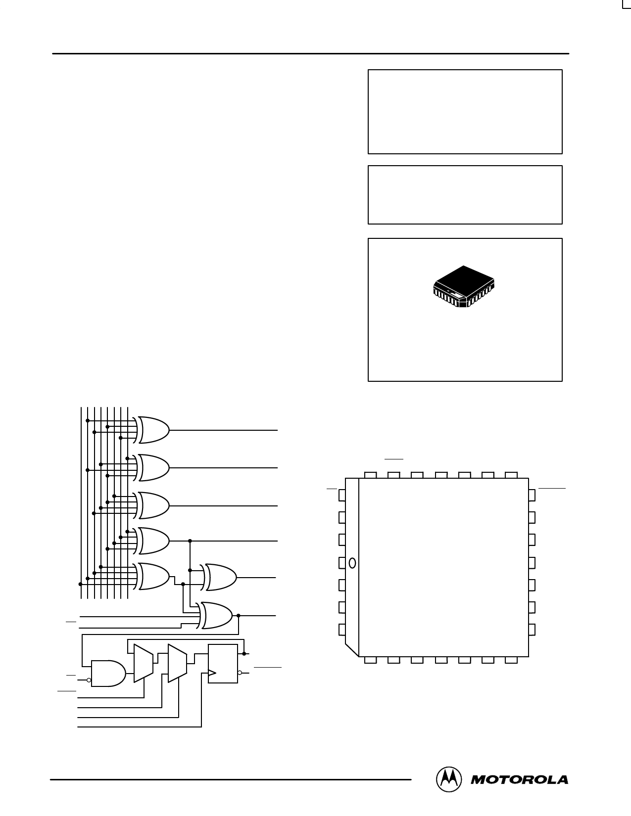
The MC10E/100E193 is an error detection and correction (EDAC)
circuit. Modified Hamming parity codes are generated on an 8-bit word
according to the pattern shown in the logic symbol. The P5 output gives
the parity of the whole word. The word parity is also provided at the PGEN
pin, after Odd/Even parity control and gating with the BPAR input. This
output also feeds to a 1-bit shiftable register, for use as part of a scan ring.
Used in conjunction with 12-bit parity generators such as the E160, a
SECDED (single error correction, double error detection) error system
can be designed for a multiple of an 8-bit word.
• Hamming Code Generation
• 8-Bit Word, Expandable
• Provides Parity of Whole Word
• Scannable Parity Register
• Extended 100E VEE Range of – 4.2V to – 5.46V
• 75kΩ Input Pulldown Resistors
MC10E193
MC100E193
ERROR DETECTION/
CORRECTION CIRCUIT
FN SUFFIX
PLASTIC PACKAGE
CASE 776-02
B INPUTS
03 6 574 2 1
BPAR
EV/OD
0
1
EN
HOLD
S-IN
SHIFT
CLK
LOGIC DIAGRAM
B2, B3, B6, B7
P2
B1, B3, B5, B7
P1
B4, B5, B6, B7
P3
B1, B2, B4, B7
P4
BYTE (B0 – B7)
P5
Pinout: 28-Lead PLCC (Top View)
EN HOLD S-IN SHIFT CLK VCCO PGEN
25 24 23 22 21 20 19
EV/OD 26
18
PARERR
BPAR 27
17 PARERR
B0 28
16 VCC
VEE 1
15 P5
B1 2
14 VCCO
PGEN
B2 3
B3 4
13 P4
12 P3
0
D
PARERR
1
PARERR
5 6 7 8 9 10 11
B4 B5 B6 B7 VCCO P1 P2
* All VCC and VCCO pins are tied together on the die.
7/96
© Motorola, Inc. 1996
2–1
REV 3
Share Link: 