MC141585 データシートの表示(PDF) - Motorola => Freescale
部品番号
コンポーネント説明
メーカー
MC141585 Datasheet PDF : 27 Pages
| |||
DC CHARACTERISTICS VDD = 5.0 V ± 5%, VSS = 0 V, TA = 25°C, Voltage Referenced to VSS
Symbol
Characteristic
Min
Typ
Max
Unit
VOH
VOL
VIL
VIH
VIL
VIH
VIL
VIH
III
III
IDD
High Level Output Voltage (R,G,B,FBKG) , Iout = – 5 mA
Low Level Output Voltage (R,G,B,FBKG), Iout = 5 mA
Digital Input Voltage (Not Including SDA and SCL)
Logic Low
Logic High
Input Voltage of Pin SDA and SCL in M_BUS Mode
Logic Low
Logic High
Input Voltage of PIXin pin
Logic Low
Logic High
High-Z Leakage Current (R, G, B and FBKG)
Input Current (HSYNC,VSYNC,RESET, SDA, SCL)
Supply Current (No Load on Any Output) at VDD=5.0V
VDD – 0.8
—
—
V
—
—
VSS + 0.4
V
—
—
0.3 VDD
V
0.7 VDD
—
—
V
—
—
0.3 VDD
V
0.7 VDD
—
—
V
—
—
1
V
4.0
—
—
V
– 10
—
+ 10
µA
– 10
—
+ 10
µA
—
—
+ 26
mA
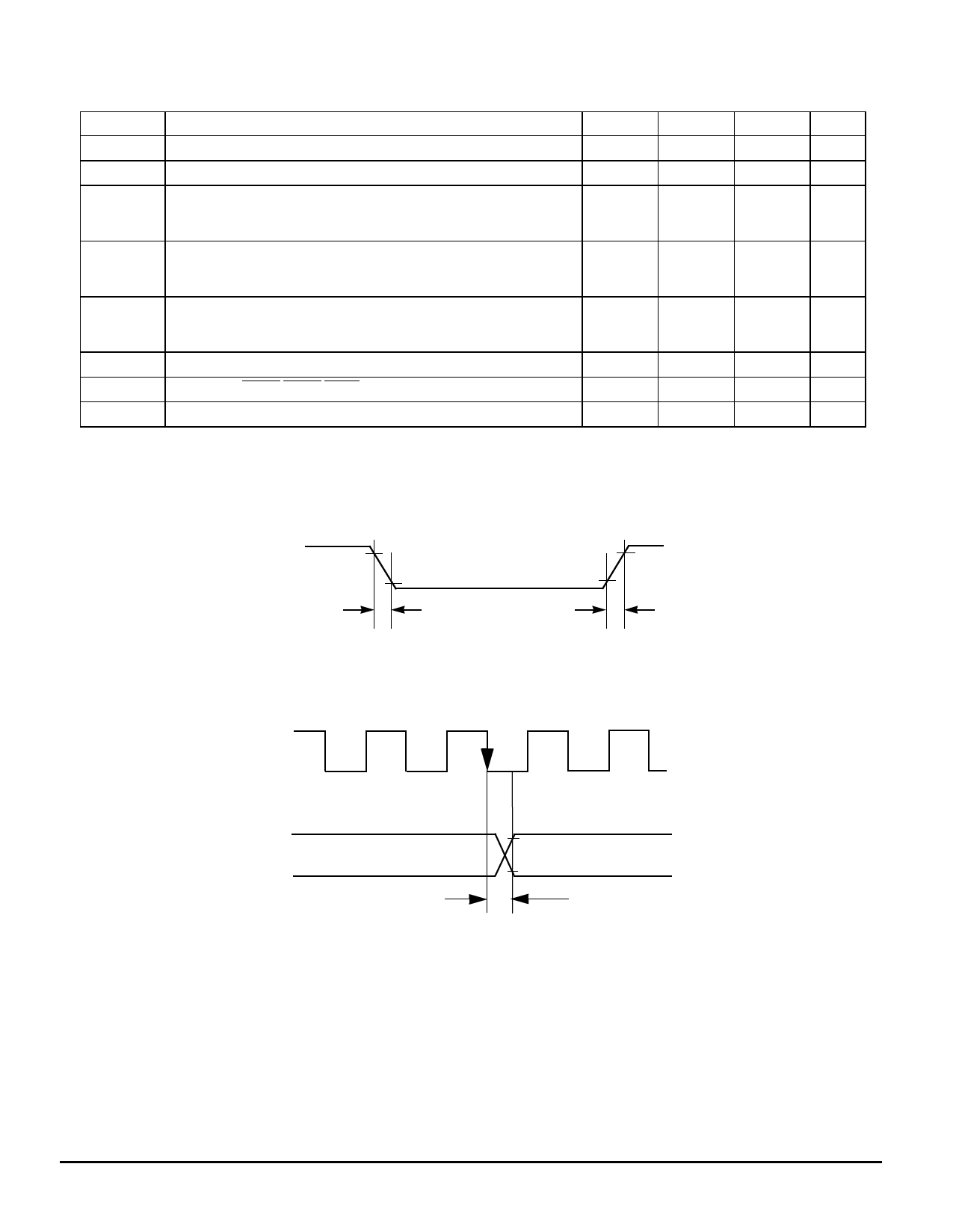
90%
10%
tf
10%
tr
90%
Figure 1. Switching Characteristics
PIXin
R,G,B,
FBKG
VDD - 0.8V
VSS + 0.4V
tpd
Figure 2. Propagation Delay Diagram
MC141585
4
MOTOROLA
Share Link: 