NLV14066BDG(2014) データシートの表示(PDF) - ON Semiconductor
部品番号
コンポーネント説明
メーカー
NLV14066BDG Datasheet PDF : 11 Pages
| |||
MC14066B
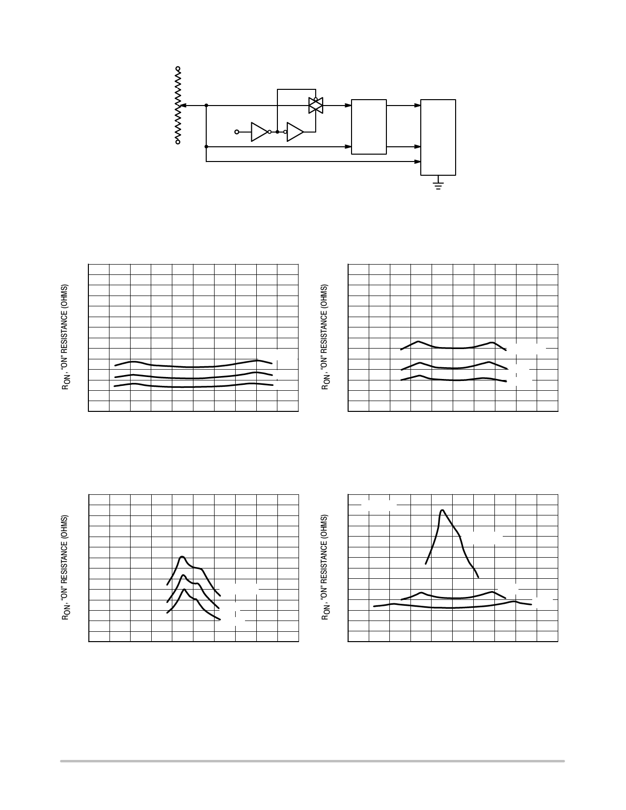
APPLICATIONS INFORMATION
Figure A illustrates use of the Analog Switch. The
0−to−5 V digital control signal is used to directly control a
5 V peak−to−peak analog signal.
The digital control logic levels are determined by VDD
and VSS. The VDD voltage is the logic high voltage, the VSS
voltage is logic low. For the example, VDD = +5 V = logic
high at the control inputs; VSS = GND = 0 V = logic low.
The maximum analog signal level is determined by VDD
and VSS. The analog voltage must not swing higher than
VDD or lower than VSS.
The example shows a 5 V peak−to−peak signal which
allows no margin at either peak. If voltage transients above
VDD and/or below VSS are anticipated on the analog
channels, external diodes (Dx) are recommended as shown
in Figure B. These diodes should be small signal types able
to absorb the maximum anticipated current surges during
clipping.
The absolute maximum potential difference between
VDD and VSS is 18 V. Most parameters are specified up to
15 V which is the recommended maximum difference
between VDD and VSS.
+5 V
VDD
VSS
5 Vp-p
SWITCH
ANALOG SIGNAL
IN
SWITCH
5 Vp-p
+5 V
OUT
ANALOG SIGNAL
EXTERNAL
CMOS
DIGITAL
CIRCUITRY
0-TO-5 V DIGITAL
CONTROL SIGNALS
MC14066B
+ 5.0 V
+ 2.5 V
GND
Figure A. Application Example
VDD
DX
SWITCH
IN
DX
SWITCH
OUT
VDD
DX
DX
VSS
VSS
Figure B. External Germanium or Schottky Clipping Diodes
http://onsemi.com
7
Share Link: 