MC33690 データシートの表示(PDF) - Freescale Semiconductor
部品番号
コンポーネント説明
メーカー
MC33690 Datasheet PDF : 26 Pages
| |||
Standalone Configuration with One-Wire Bus
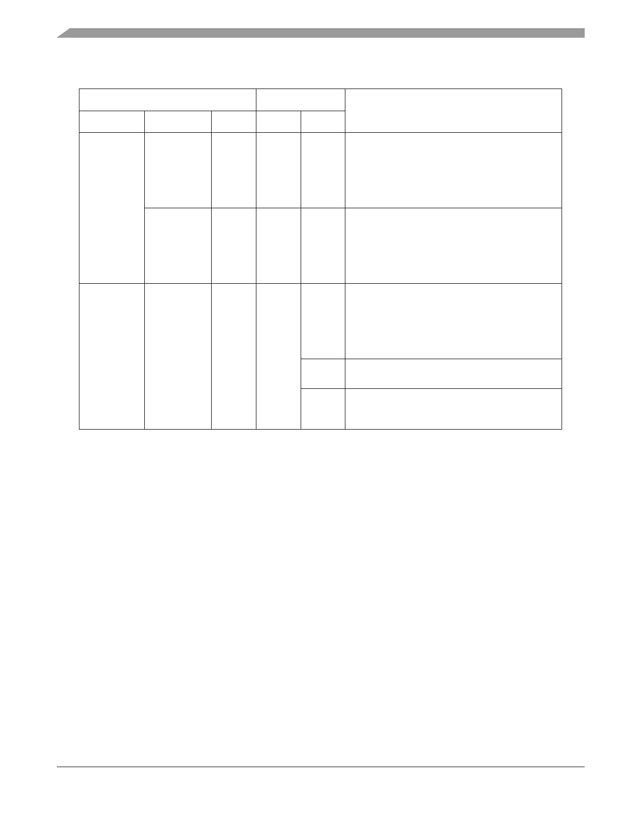
Table 4. Communication Modes Description
Configuration
Type
Bus Type
Configuration Pins
Name Mode1 Mode2
Pin Status Function Description
Standalone 1 wire (VBAT) A
0
0 K output/input:
• demodulator output
• amplitude modulation input
• shutdown/wake-up
AM must be connected to VSUP
DOUT forces a low level
2 wires (VBAT) B
0
1 K output:
• demodulator output
AM input:
• amplitude modulation input
• shutdown/wake-up
DOUT forces a low level
Direct
2 wires (VDD)
C
1
x DOUT output:
Connection to
• demodulator output
a MCU
AM input:
• amplitude modulation input
MODE2 input:
• shutdown/wake-up
1 K output/input (standalone ISO 9141 interface):
• driven by Tx and monitored by Rx
0 K input (standalone ISO 9141 interface):
• monitored by Rx
• Tx disabled
7 Standalone Configuration with One-Wire Bus
When a low level is applied on pins MODE1 and MODE2, the circuit is in configuration A (see Figure 24). After power on, the
circuit is set into read mode. The demodulator output is directly routed to the ISO 9141 interface output K.
The circuit can be set into write mode at anytime by violation of all possible patterns on the single wire bus during more than
1ms. Then, the K line achieves the amplitude modulation by switching on/off both antenna drivers.
After 1ms of inactivity at the end of the challenge phase (bus in idle recessive one state), the circuit is set back into read mode.
The circuit can be put into standby mode by forcing the K line at zero during more than 2 ms after entering the write mode.
After the K line is released, the circuit sends an acknowledge pulse before entering into standby mode. In standby mode, the
oscillator and most of the internal biasing currents are switched off. Therefore, the functions (tag reader, ISO 9141 driver) are
inactive except the voltage regulator and the ISO 9141 receiver on pin K. The driver output TD1 forces a low level and TD2
forces a high level. A rising edge on K wakes up the circuit. After completion of the wake-up sequence, the circuit is
automatically set in read mode.
In configuration A, DOUT and Rx outputs always force a low level and Tx is disabled.
MC33690 Standalone Tag Reader Circuit, Rev. 5
10
Freescale Semiconductor
Share Link: 