MC74AC273DWR2G(2016) データシートの表示(PDF) - ON Semiconductor
部品番号
コンポーネント説明
メーカー
MC74AC273DWR2G Datasheet PDF : 8 Pages
| |||
MC74AC273, MC74ACT273
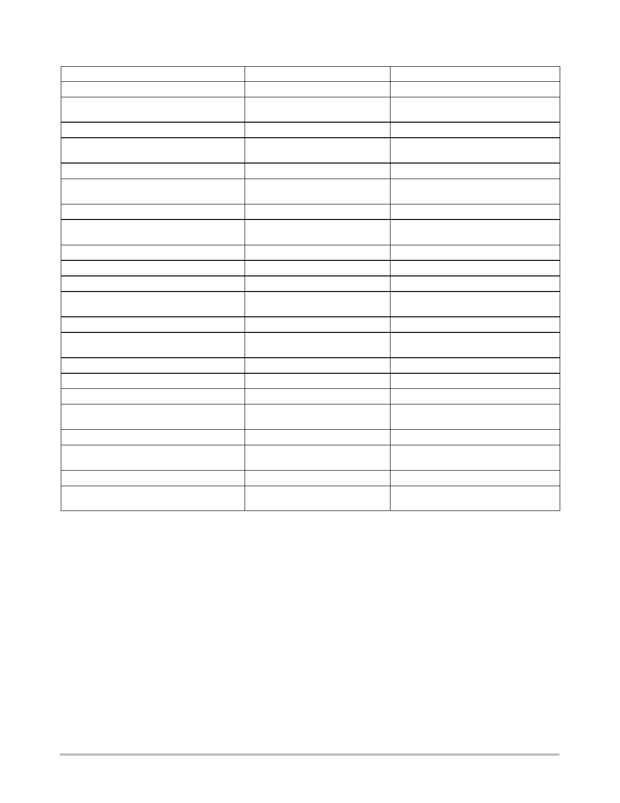
DC CHARACTERISTICS
74ACT
74ACT
Symbol
Parameter
VIH
Minimum High Level Input Voltage
VIL
Maximum Low Level Input Voltage
VOH
Minimum High Level Output Voltage
VCC
(V)
TA = +25°C
TA =
−40°C to +85°C
Typ
Guaranteed Limits
4.5 1.5 2.0
2.0
5.5 1.5 2.0
2.0
4.5 1.5 0.8
0.8
5.5 1.5 0.8
0.8
4.5 4.49 4.4
4.4
5.5 5.49 5.4
5.4
4.5
− 3.86
3.76
5.5
− 4.86
4.76
VOL
Maximum Low Level Output Voltage
4.5 0.001 0.1
0.1
5.5 0.001 0.1
0.1
4.5
− 0.36
0.44
5.5
− 0.36
0.44
IIN
Maximum Input Leakage Current
5.5
− ±0.1
±1.0
DICCT Additional Max. ICC/Input
5.5 0.6
−
1.5
IOLD
†Minimum Dynamic Output Current
5.5
−
−
75
IOHD
5.5
−
−
−75
ICC
Maximum Quiescent Supply Current
5.5
−
8.0
80
*All outputs loaded; thresholds on input associated with output under test.
†Maximum test duration 2.0 ms, one output loaded at a time.
Unit
Conditions
V
VOUT = 0.1 V
or VCC − 0.1 V
V
VOUT = 0.1 V
or VCC − 0.1 V
V
IOUT = −50 mA
*VIN = VIL or VIH
V
IOH −24 mA
−24 mA
V
IOUT = 50 mA
*VIN = VIL or VIH
V
24 mA
IOL 24 mA
mA
VI = VCC, GND
mA
VI = VCC − 2.1 V
mA
VOLD = 1.65 V Max
VOHD = 3.85 V Min
mA
VIN = VCC or GND
AC CHARACTERISTICS (For Figures and Waveforms − See Section 3 of the ON Semiconductor FACT Data Book, DL138/D)
Symbol
Parameter
fmax
Maximum Clock Frequency
tPHL
Propagation Delay Clock to Output
tPLH
Propagation Delay Clock to Output
tPHL
Propagation Delay MR to Output
*Voltage Range 5.0 V is 5.0 V ±0.5 V.
VCC*
(V)
5.0
5.0
5.0
5.0
74ACT
TA = +25°C CL = 50 pF
Min Typ Max
125 200
−
3.0 6.0 10
3.0 6.5 11
3.0 7.0 11
74ACT
TA = −40°C to +85°C
CL = 50 pF
Min
Max
125
−
2.5
11.0
2.5
12.0
2.5
11.5
Unit
MHz
ns
ns
ns
Figure
No.
3−3
3−6
3−6
3−6
AC OPERATING REQUIREMENTS
74ACT
74ACT
Symbol
Parameter
ts
Setup Time, HIGH or LOW − Data to CP
th
Hold Time, HIGH or LOW − Data to CP
tw
Clock Pulse Width − HIGH or LOW
tw
MR Pulse Width − HIGH or LOW
trec
Recovery Time − MR to CP
*Voltage Range 5.0 V is 5.0 V ±0.5 V.
VCC*
(V)
5.0
5.0
5.0
5.0
5.0
TA = +25°C CL = 50 pF
TA = −40°C to +85°C
CL = 50 pF
Typ
Guaranteed Minimum
3.0
4.5
5.0
−2.5
2.0
2.0
2.5
4.0
4.5
2.5
4.0
4.5
−1.0
2.0
3.0
Unit
ns
ns
ns
ns
ns
Figure
No.
3−9
3−9
3−6
3−6
3−6
CAPACITANCE
Symbol
Parameter
CIN
Input Capacitance
CPD
Power Dissipation Capacitance
Value Typ
Unit
4.5
pF
50
pF
Test Conditions
VCC = 5.0 V
VCC = 5.0 V
www.onsemi.com
5
Share Link: 