MC74HC4046ADTR2G データシートの表示(PDF) - ON Semiconductor
部品番号
コンポーネント説明
メーカー
MC74HC4046ADTR2G Datasheet PDF : 18 Pages
| |||
MC74HC4046A
[VCO Section]
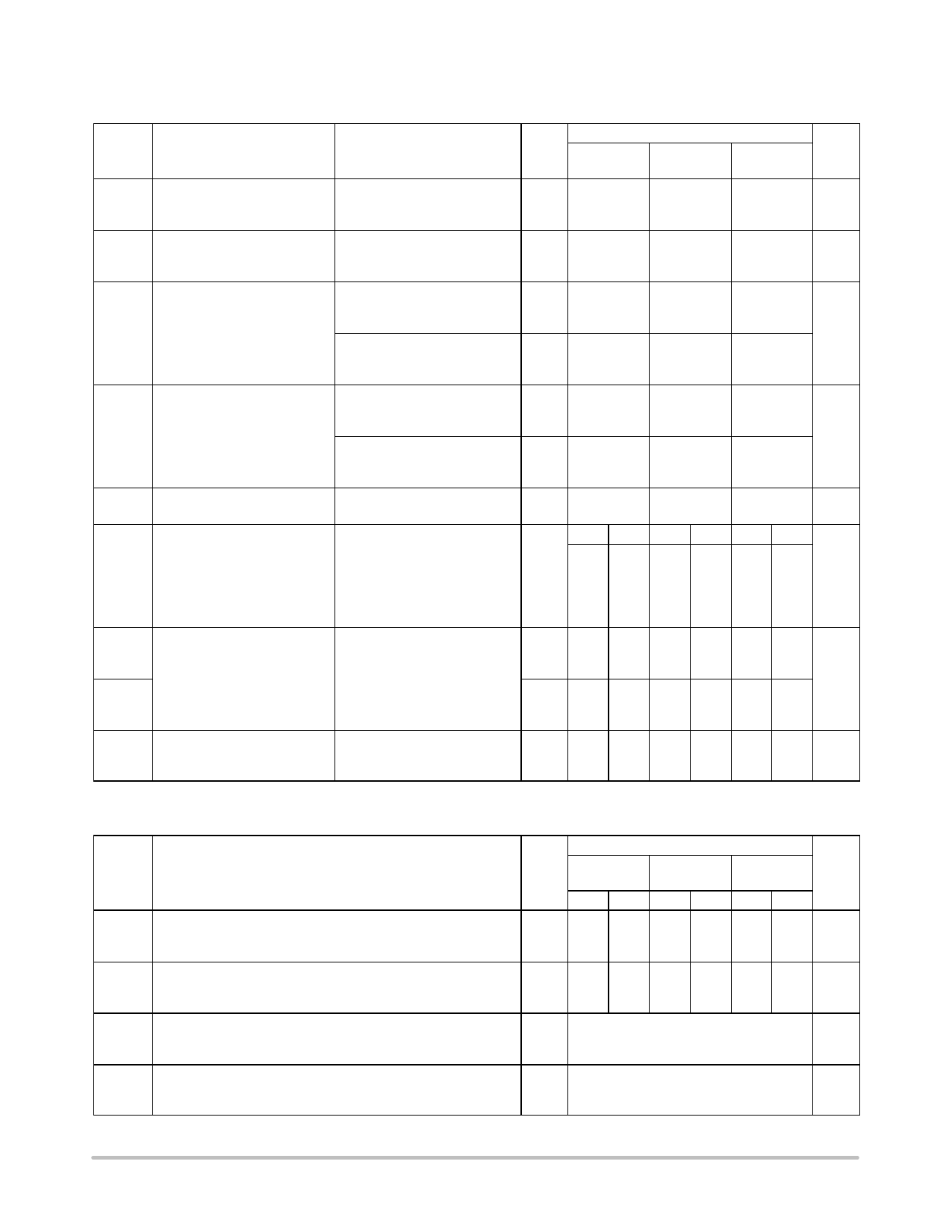
DC ELECTRICAL CHARACTERISTICS (Voltages Referenced to GND)
Symbol
VIH
Parameter
Minimum High−Level
Input Voltage
INH
Test Conditions
Vout = 0.1 V or VCC − 0.1 V
|Iout| ≤ 20 mA
Guaranteed Limit
VCC
– 55 to
V
25_C
≤ 85°C
≤ 125°C Unit
3.0
2.1
2.1
2.1
V
4.5
3.15
3.15
3.15
6.0
4.2
4.2
4.2
VIL Maximum Low−Level
Input Voltage
INH
Vout = 0.1 V or VCC − 0.1 V
3.0
0.90
|Iout| ≤ 20 mA
4.5
1.35
6.0
1.8
0.9
1.35
1.8
0.9
V
1.35
1.8
VOH Minimum High−Level
Output Voltage
VCOOUT
VOL Maximum Low−Level
Output Voltage
VCOOUT
Iin
Maximum Input Leakage
Current INH, VCOIN
Vin = VIH or VIL
|Iout| ≤ 20 mA
Vin = VIH or VIL
|Iout| ≤ 4.0 mA
|Iout| ≤ 5.2 mA
Vout = 0.1 V or VCC − 0.1 V
|Iout| ≤ 20 mA
Vin = VIH or VIL
|Iout| ≤ 4.0 mA
|Iout| ≤ 5.2 mA
Vin = VCC or GND
3.0
1.9
1.9
1.9
V
4.5
4.4
4.4
4.4
6.0
5.9
5.9
5.9
4.5
3.98
3.84
6.0
5.48
5.34
3.0
0.1
0.1
4.5
0.1
0.1
6.0
0.1
0.1
3.7
5.2
0.1
V
0.1
0.1
4.5
0.26
0.33
6.0
0.26
0.33
6.0
0.1
1.0
0.4
0.4
1.0
mA
Min Max Min Max Min Max
VVCO IN
Operating Voltage Range at
VCOIN over the range
specified for R1; For linearity
see Fig. 15A, Parallel value of
R1 and R2 should be > 2.7 kW
INH = VIL
3.0 0.1 1.0 0.1 1.0 0.1 1.0 V
4.5 0.1 2.5 0.1 2.5 0.1 2.5
6.0 0.1 4.0 0.1 4.0 0.1 4.0
R1 Resistor Range
3.0 3.0 300 3.0 300 3.0 300 kW
4.5 3.0 300 3.0 300 3.0 300
6.0 3.0 300 3.0 300 3.0 300
R2
3.0 3.0 300 3.0 300 3.0 300
4.5 3.0 300 3.0 300 3.0 300
6.0 3.0 300 3.0 300 3.0 300
C1 Capacitor Range
3.0 40 No
pF
4.5 40 Limit
6.0 40
[VCO Section]
AC ELECTRICAL CHARACTERISTICS (CL = 50 pF, Input tr = tf = 6.0 ns)
VCC
Symbol
Parameter
V
Df/T Frequency Stability with
3.0
Temperature Changes
4.5
(Figure 14A, B, C)
6.0
fo VCO Center Frequency
3.0
(Duty Factor = 50%)
4.5
(Figure 15A, B, C, D)
6.0
DfVCO VCO Frequency Linearity
3.0
4.5
6.0
∂ VCO Duty Factor at VCOOUT
3.0
4.5
6.0
Guaranteed Limit
– 55 to
25_C
≤ 85°C
≤ 125°C
Min Max Min Max Min Max
3
11
13
See Figures 16A, B, C
Typical 50%
Unit
%/K
MHz
%
%
http://onsemi.com
4
Share Link: 