74HC541 データシートの表示(PDF) - ON Semiconductor
部品番号
コンポーネント説明
メーカー
74HC541 Datasheet PDF : 10 Pages
| |||
MC74HC541A
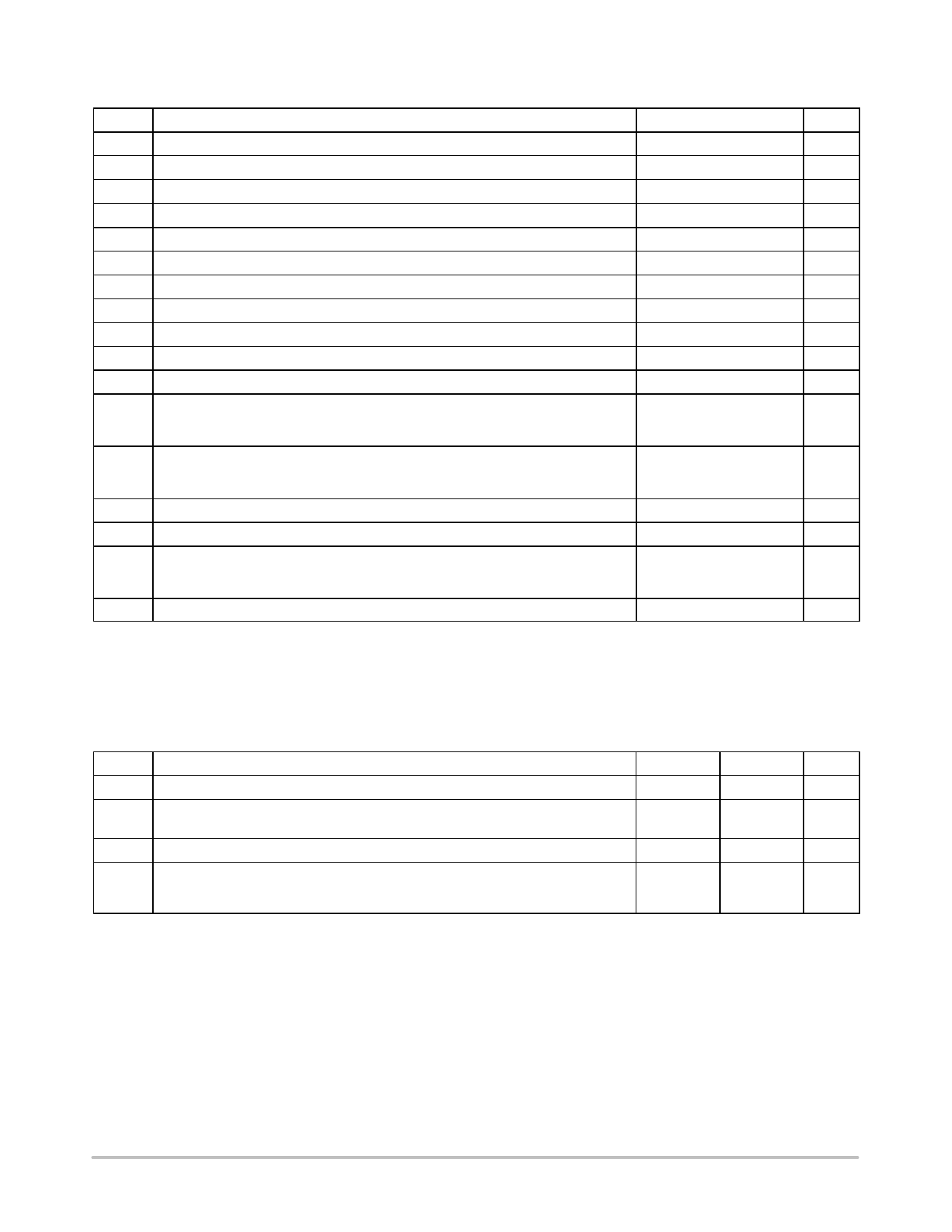
MAXIMUM RATINGS
Symbol
Parameter
Value
VCC
VI
VO
IIK
IOK
IO
ICC
IGND
TSTG
TL
TJ
qJA
DC Supply Voltage
DC Input Voltage
DC Output Voltage (Note 1)
DC Input Diode Current
DC Output Diode Current
DC Output Sink Current
DC Supply Current per Supply Pin
DC Ground Current per Ground Pin
Storage Temperature Range
Lead Temperature, 1 mm from Case for 10 Seconds
Junction Temperature under Bias
Thermal Resistance
PDIP
SOIC
TSSOP
*0.5 to )7.0
*0.5 v VI v )0.5
*0.5 v VO v )0.5
$20
$35
$35
$75
$75
*65 to )150
260
)150
67
96
128
PD Power Dissipation in Still Air at 85_C
PDIP
750
SOIC
500
TSSOP
450
MSL Moisture Sensitivity
Level 1
FR
VESD
Flammability Rating
ESD Withstand Voltage
Oxygen Index: 30% − 35%
Human Body Model (Note 2)
Machine Model (Note 3)
Charged Device Model (Note 4)
UL 94 V−0 @ 0.125 in
> 4000
> 300
> 1000
ILatchup Latchup Performance
Above VCC and Below GND at 85_C (Note 5)
$300
1. IO absolute maximum rating must be observed.
2. Tested to EIA/JESD22−A114−A.
3. Tested to EIA/JESD22−A115−A.
4. Tested to JESD22−C101−A.
5. Tested to EIA/JESD78.
6. For high frequency or heavy load considerations, see the ON Semiconductor High−Speed CMOS Data Book (DL129/D).
Unit
V
V
V
mA
mA
mA
mA
mA
_C
_C
_C
_C/W
mW
V
mA
RECOMMENDED OPERATING CONDITIONS
Symbol
Parameter
Min
Max
Unit
ÎÎÎÎÎÎÎÎÎÎÎÎÎÎÎÎÎÎÎÎÎÎÎÎÎÎÎÎÎÎÎÎÎ VCC
ÎÎÎÎÎÎÎÎÎÎÎÎÎÎÎÎÎÎÎÎÎÎÎÎÎÎÎÎÎÎÎÎÎ VIN,
VOUT
DC Supply Voltage
DC Input Voltage, Output Voltage
(Referenced to GND)
2.0
(Referenced to GND)
0
6.0
V
VCC
V
ÎÎÎÎÎÎÎÎÎÎÎÎÎÎÎÎÎÎÎÎÎÎÎÎÎÎÎÎÎÎÎÎÎ TA
Operating Temperature Range, All Package Types
*55
)125
_C
ÎÎÎÎÎÎÎÎÎÎÎÎÎÎÎÎÎÎÎÎÎÎÎÎÎÎÎÎÎÎÎÎÎ tr, tf Input Rise/Fall Time
ÎÎÎÎÎÎÎÎÎÎÎÎÎÎÎÎÎÎÎÎÎÎÎÎÎÎÎÎÎÎÎÎÎÎÎÎÎÎÎÎÎÎÎÎÎÎÎÎÎÎÎÎÎÎÎÎÎÎÎÎÎÎÎÎÎÎ (Figure 3)
VCC = 2.0 V
0
VCC = 4.5 V
0
VCC = 6.0 V
0
1000
ns
500
400
ÎÎÎÎÎÎÎÎÎÎÎÎÎÎÎÎÎÎÎÎÎÎÎÎÎÎÎÎÎÎÎÎÎ 7. Unused inputs may not be left open. All inputs must be tied to a high−logic voltage level or a low−logic input voltage level.
http://onsemi.com
3
Share Link: 