MC74LVX541_14 データシートの表示(PDF) - ON Semiconductor
部品番号
コンポーネント説明
メーカー
MC74LVX541_14 Datasheet PDF : 7 Pages
| |||
MC74LVX541
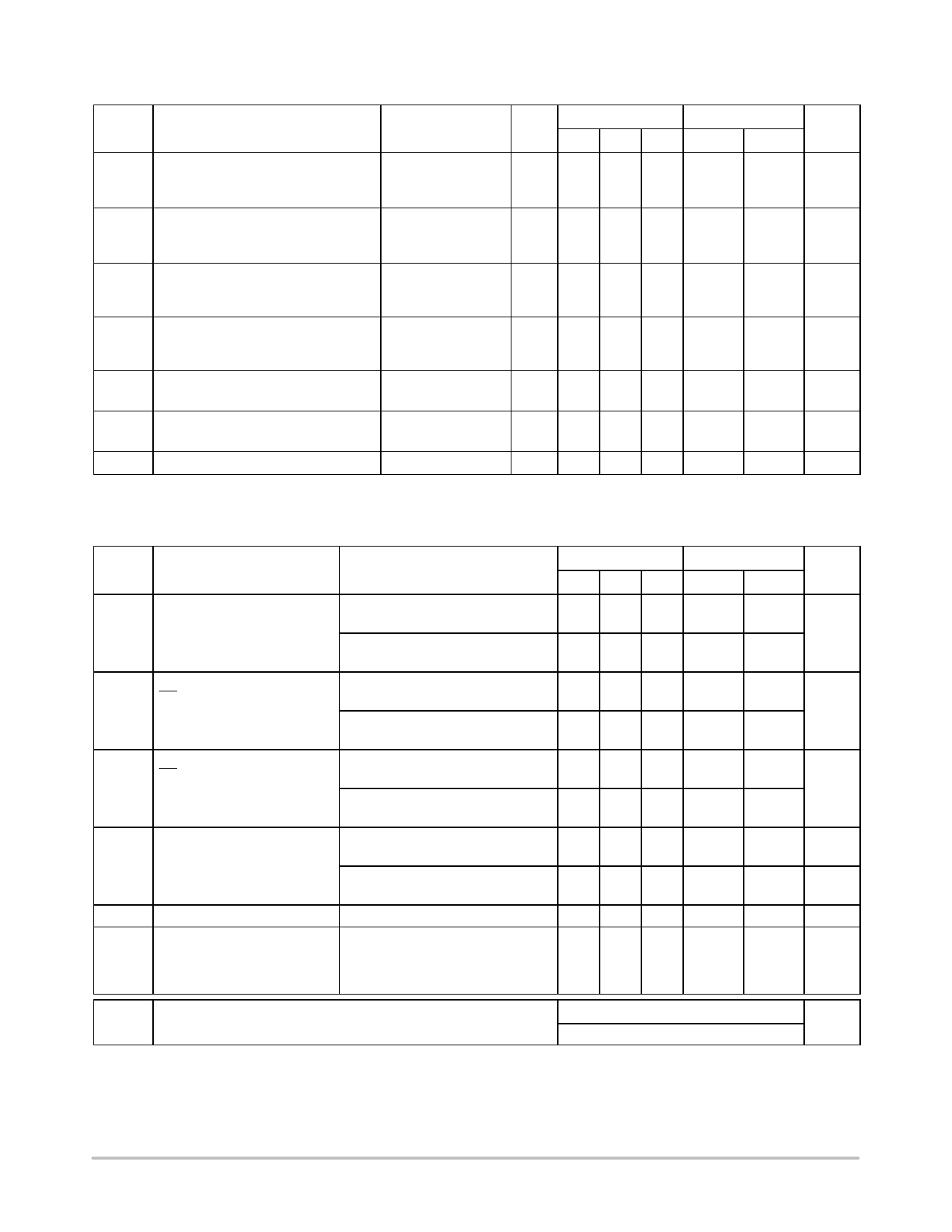
DC ELECTRICAL CHARACTERISTICS
Symbol
Parameter
VCC
TA = 25°C
TA = −40 to 85°C
Test Conditions
V Min Typ Max Min
Max
Unit
VIH Minimum High−Level Input Voltage
2.0 1.50
3.0 2.0
3.6 2.4
1.50
V
2.0
2.4
VIL Maximum Low−Level Input Voltage
2.0
0.50
0.50
V
3.0
0.80
0.80
3.6
0.80
0.80
VOH Minimum High−Level Output Voltage IOH = −50 mA
2.0 1.9 2.0
1.9
V
Vin = VIH or VIL
IOH = −50 mA
3.0 2.9 3.0
2.9
IOH = −4 mA
3.0 2.58
2.48
VOL Maximum Low−Level Output Voltage IOL = 50 mA
Vin = VIH or VIL
IOL = 50 mA
IOL = 4 mA
2.0
0.0 0.1
3.0
0.0 0.1
3.0
0.36
0.1
V
0.1
0.44
Iin
Maximum Input Leakage Current
Vin = 5.5 V or GND
0 to
3.6
±0.1
±1.0
mA
IOZ Maximum Three−State Leakage
Current
Vin = VIL or VIH
3.6
Vout = VCC or GND
±0.2
±2.5
mA
5
ICC Maximum Quiescent Supply Current Vin = VCC or GND
3.6
4.0
40.0
mA
Product parametric performance is indicated in the Electrical Characteristics for the listed test conditions, unless otherwise noted. Product
performance may not be indicated by the Electrical Characteristics if operated under different conditions.
AC ELECTRICAL CHARACTERISTICS (Input tr = tf = 3.0 ns)
Symbol
tPLH,
tPHL
Parameter
Maximum Propagation Delay,
A to Y
tPZL,
tPZH
Output Enable TIme,
OE to Y
tPLZ,
tPHZ
Output Disable Time,
OE to Y
tOSLH, Output to Output Skew
tOSHL
Cin Maximum Input Capacitance
Cout Maximum Three−State Output
Capacitance
(Output in High Impedance
State)
Test Conditions
VCC = 2.7 V
VCC = 3.3 ± 0.3 V
VCC = 2.7 V
RL = 1 kW
VCC = 3.3 ± 0.3 V
RL = 1 kW
VCC = 2.7 V
RL = 1 kW
VCC = 3.3 ± 0.3 V
RL = 1 kW
VCC = 2.7 V
(Note 1)
CL = 15 pF
CL = 50 pF
CL = 15 pF
CL = 50 pF
CL = 15 pF
CL = 50 pF
CL = 15 pF
CL = 50 pF
CL = 50 pF
CL = 50 pF
CL = 50 pF
VCC = 3.3 ± 0.3 V
(Note 1)
CL = 50 pF
TA = 25°C
TA = −40 to 85°C
Min Typ Max Min
Max
Unit
5.0 7.0
1.0
8.5
ns
7.5 10.5 1.0
12.0
3.5 5.0
1.0
6.0
5.0 7.0
1.0
8.0
6.8 10.5 1.0
12.5
ns
9.3 14.0 1.0
16.0
4.7 7.2
1.0
8.5
6.2 9.2
1.0
10.5
11.2 15.4 1.0
17.5
ns
6.0 8.8
1.0
10.0
1.5
1.5
ns
1.0
1.0
ns
4.0 10
6.0
10
pF
pF
Typical @ 25°C, VCC = 5.0 V
CPD Power Dissipation Capacitance (Note 2)
18
pF
1. Parameter guaranteed by design. tOSLH = |tPLHm − tPLHn|, tOSHL = |tPHLm − tPHLn|.
2. CPD is defined as the value of the internal equivalent capacitance which is calculated from the operating current consumption without load.
Average operating current can be obtained by the equation: ICC(OPR) = CPD VCC fin + ICC / 8 (per bit). CPD is used to determine the no−load
dynamic power consumption; PD = CPD VCC2 fin + ICC VCC.
http://onsemi.com
3
Share Link: 