MCF51JF128(2011) データシートの表示(PDF) - Freescale Semiconductor
部品番号
コンポーネント説明
メーカー
MCF51JF128 Datasheet PDF : 71 Pages
| |||
Nonswitching electrical specifications
Symbol
TA
VDD
Description
Ambient temperature
3.3 V supply voltage
Value
25
3.3
Unit
°C
V
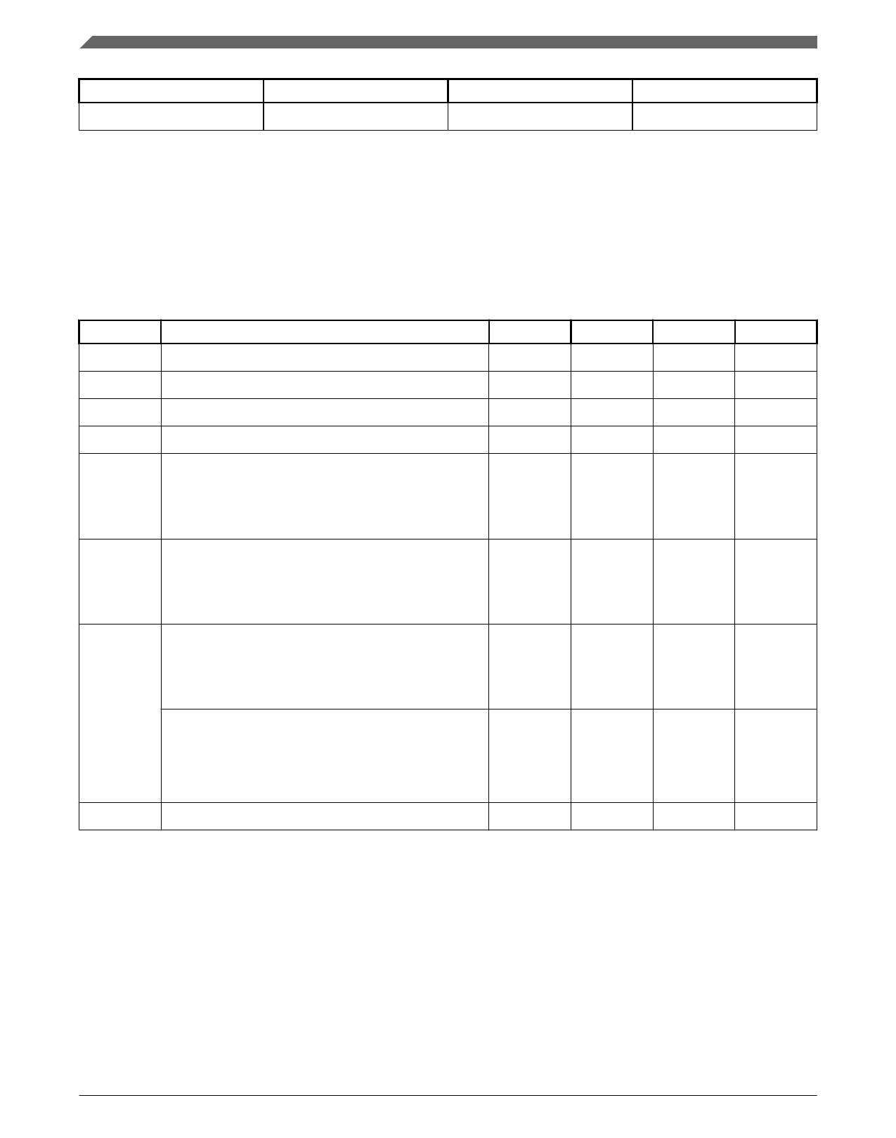
5.2 Nonswitching electrical specifications
5.2.1 Voltage and Current Operating Requirements
Table 1. Voltage and current operating requirements
Symbol Description
VDD
Supply voltage
VDDA
Analog supply voltage
VDD – VDDA VDD-to-VDDA differential voltage
VSS – VSSA VSS-to-VSSA differential voltage
VIH
Input high voltage
• 2.7 V ≤ VDD ≤ 3.6 V
• 1.7 V ≤ VDD ≤ 2.7 V
Min.
Max.
Unit
1.71
3.6
V
1.71
3.6
V
–0.1
0.1
V
–0.1
0.1
V
0.7 × VDD
—
V
0.75 × VDD
—
V
Notes
1
VIL
Input low voltage
• 2.7 V ≤ VDD ≤ 3.6 V
• 1.7 V ≤ VDD ≤ 2.7 V
2
—
0.35 × VDD
V
—
0.3 × VDD
V
IIC
DC injection current — single pin
• VIN > VDD
• VIN < VSS
3
0
2
mA
0
–0.2
mA
DC injection current — total MCU limit, includes sum
3
of all stressed pins
• VIN > VDD
• VIN < VSS
0
25
mA
0
–5
mA
VRAM
VDD voltage required to retain RAM
1.2
—
V
1. The device always interprets an input as a 1 when the input is greater than or equal to VIH (min.) and less than or equal to
VIH (max.), regardless of whether input hysteresis is turned on.
2. The device always interprets an input as a 0 when the input is less than or equal to VIL (max.) and greater than or equal to
VIL (min.), regardless of whether input hysteresis is turned on.
3. All functional non-supply pins are internally clamped to VSS and VDD. Input must be current limited to the value specified.
To determine the value of the required current-limiting resistor, calculate resistance values for positive and negative clamp
voltages, then use the larger of the two values. Power supply must maintain regulation within operating VDD range during
instantaneous and operating maximum current conditions. If positive injection current (VIn > VDD) is greater than IDD, the
injection current may flow out of VDD and could result in external power supply going out of regulation. Ensure external
VDD load will shunt current greater than maximum injection current. This will be the greatest risk when the MCU is not
MCF51JF128 Advance Information Data Sheet, Rev. 2, 05/2011.
10
Preliminary
Freescale Semiconductor, Inc.
Share Link: 