MCP1253 データシートの表示(PDF) - Microchip Technology
部品番号
コンポーネント説明
メーカー
MCP1253 Datasheet PDF : 20 Pages
| |||
5.1 Capacitor Selection
The style and value of capacitors used with the
MCP1252 and MCP1253 family of devices determine
several important parameters such as output voltage
ripple and charge pump strength. To minimize noise
and ripple, it is recommended that low ESR (0.1 )
capacitors be used for both CIN and COUT. These
capacitors should be either ceramic or tantalum and
should be 10 µF or higher. Aluminum capacitors are not
recommended because of their high ESR.
If the source impedance to VIN is very low, up to several
megahertz, CIN may not be required. Alternatively, a
somewhat smaller value of CIN may be substituted for
the recommended 10 µF, but will not be as effective in
preventing ripple on the VIN pin.
The value of COUT controls the amount of output volt-
age ripple present on VOUT. Increasing the size of
COUT will reduce output ripple at the expense of a
slower turn-on time from shutdown and a higher in-rush
current.
The flying capacitor (CFLY) controls the strength of the
charge pump. In order to achieve the maximum rated
output current (120 mA), it is necessary to have at least
1 µF of capacitance for the flying capacitor. A smaller
flying capacitor delivers less charge per clock cycle to
the output capacitor, resulting in lower output ripple.
The output ripple is reduced at the expense of maxi-
mum output current and efficiency.
5.2 Output Voltage Setting
The MCP1252-33X50 and MCP1253-33X50 feedback
controllers select between an internally-set, regulated
output voltage (3.3V or 5.0V). Connect SELECT to
GND for a regulated 5.0V output and connect SELECT
to VIN for a regulated 3.3V output.
The MCP1252-ADJ and MCP1253-ADJ utilize an
external resistor divider that allows the output voltage
to be adjusted between 1.5V and 5.5V. For an adjust-
able output, connect a resistor between VOUT and FB
(R1) and another resistor between FB and GND (R2). In
the following equation, choose R2 to be less than or
equal to 30 k and calculate R1 from the following
formula:
EQUATION
R1 = R2VOUT VFB – 1
and
EQUATION
VOUT = VFB1 + R1 R2
where:
VOUT is the desired output voltage from 1.5V to 5.5V
VFB is the internal regulation voltage, nominally 1.21V
MCP1252/3
Note that the tolerance of the external resistors will
have an effect on the accuracy of the output voltage.
For optimum results, it is recommended that the
external resistors have a tolerance no larger than 1%.
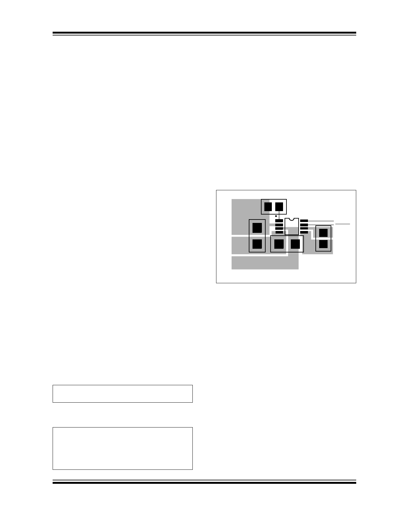
5.3 Recommended Layout
The MCP1252 and MCP1253 family of devices transfer
charge at high switching frequencies, producing fast,
high peak, transient currents. As a result, any stray
inductance in the component layout will produce
unwanted noise in the system. Proper board layout
techniques are required to ensure optimum perfor-
mance. Figure 5-3 depicts the recommended board
layout. The input capacitor connected between VIN and
GND, and the output capacitor connected between
VOUT and GND, are 10 µF ceramic, X7R dielectric, in
1206 packages. The flying capacitor connected
between C+ and C- is a 1 µF ceramic, X7R dielectric in
a 0805 package. The layout is scaled 3:1.
VOUT
GND
VIN
PGOOD
SELECT
SHDN
C+
C-
FIGURE 5-3:
Recommended Printed
Circuit Board Layout.
2002-2013 Microchip Technology Inc.
DS21752B-page 11
Share Link: 