MCP121-240I データシートの表示(PDF) - Microchip Technology
部品番号
コンポーネント説明
メーカー
MCP121-240I Datasheet PDF : 28 Pages
| |||
MCP102/103/121/131
1.0 ELECTRICAL
CHARACTERISTICS
Absolute Maximum Ratings†
VDD . . . . . . . . . . . . . . . . . . . . . . . . . . . . . . . . . . . . . . . . . 7.0V
Input current (VDD) . . . . . . . . . . . . . . . . . . . . . . . . . . . .10 mA
Output current (RST) . . . . . . . . . . . . . . . . . . . . . . . . . .10 mA
Rated Rise Time of VDD . . . . . . . . . . . . . . . . . . . . . . 100V/µs
All inputs and outputs (except RST) w.r.t. VSS
. . . . . . . . . . . . . . . . . . . . . . . . . . . . . . . -0.6V to (VDD + 1.0V)
RST output w.r.t. VSS . . . . . . . . . . . . . . . . . . . -0.6V to 13.5V
Storage temperature . . . . . . . . . . . . . . . . . . -65°C to + 150°C
Ambient temp. with power applied . . . . . . . -40°C to + 125°C
Maximum Junction temp. with power applied . . . . . . . . 150°C
ESD protection on all pins . . . . . . . . . . . . . . . . . . . . . . . . . ≥ 2 kV
† Notice: Stresses above those listed under “Maximum
Ratings” may cause permanent damage to the device. This is
a stress rating only and functional operation of the device at
those or any other conditions above those indicated in the
operational listings of this specification is not implied.
Exposure to maximum rating conditions for extended periods
may affect device reliability.
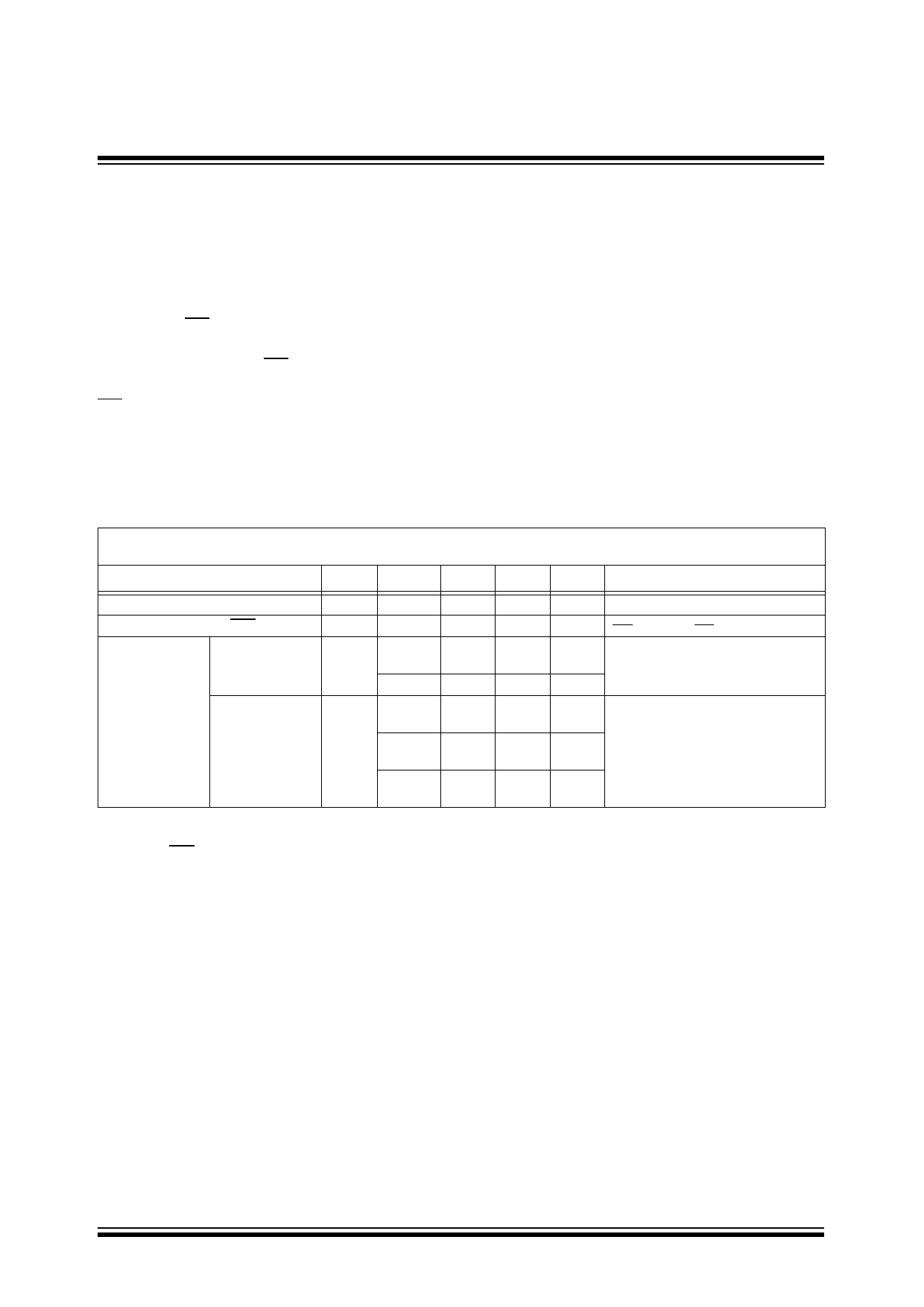
DC CHARACTERISTICS
Electrical Specifications: Unless otherwise indicated, all limits are specified for: VDD = 1V to 5.5V, RPU = 100 kΩ (MCP121 only),
TA = -40°C to +125°C.
Parameters
Sym
Min
Typ
Max Units
Conditions
Operating Voltage Range
Specified VDD Value to RST low
Operating Current
MCP102,
MCP103,
VDD
1.0
VDD
1.0
IDD
—
—
5.5
V
—
V IRST = 10 uA, VRST < 0.2V
<1
1.75
µA Reset Power-up Timer (tRPU) Inactive
MCP121
MCP131
—
—
20.0
µA Reset Power-up Timer (tRPU) Active
IDD
—
<1
1.75
µA VDD > VTRIP and Reset Power-up
Timer (tRPU) Inactive
—
—
75
µA VDD < VTRIP and Reset Power-up
Timer (tRPU) Inactive (Note 3)
—
—
90
µA Reset Power-up Timer (tRPU) Active
(Note 4)
Note 1:
2:
3:
4:
5:
6:
Trip point is ±1.5% from typical value.
Trip point is ±2.5% from typical value.
RST output is forced low. There is a current through the internal pull-up resistor.
This includes the current through the internal pull-up resistor and the reset power-up timer.
This specification allows this device to be used in PICmicro® microcontroller applications that require In-Circuit Serial
Programming™ (ICSP™) (see device-specific programming specifications for voltage requirements). This specification
DOES NOT allow a continuos high voltage to be present on the open-drain output pin (VOUT). The total time that the
VOUT pin can be above the maximum device operational voltage (5.5V) is 100s. Current into the VOUT pin should be
limited to 2 mA and it is recommended that the device operational temperature be maintained between 0°C to 70°C
(+25°C preferred). For additional information, please refer to Figure 2-33.
This parameter is established by characterization and not 100% tested.
DS21906B-page 2
© 2005 Microchip Technology Inc.
Share Link: 