MCP73827-4.2 データシートの表示(PDF) - Microchip Technology
部品番号
コンポーネント説明
メーカー
MCP73827-4.2
Microchip Technology

MCP73827-4.2 Datasheet PDF : 20 Pages
| |||
MCP73827
1.0 ELECTRICAL
CHARACTERISTICS
1.1 Maximum Ratings*
VIN...................................................................... -0.3V to 6.0V
All inputs and outputs w.r.t. GND ................-0.3 to (VIN+0.3)V
Current at MODE Pin .............................................. +/-30 mA
Current at VDRV.......................................................... +/-1 mA
Maximum Junction Temperature, TJ.............................. 150°C
Storage temperature .....................................-65°C to +150°C
ESD protection on all pins ..................................................≥ 4 kV
*Notice: Stresses above those listed under “Maximum
Ratings” may cause permanent damage to the device.
This is a stress rating only and functional operation of
the device at those or any other conditions above those
indicated in the operational listings of this specification
is not implied. Exposure to maximum rating conditions
for extended periods may affect device reliability.
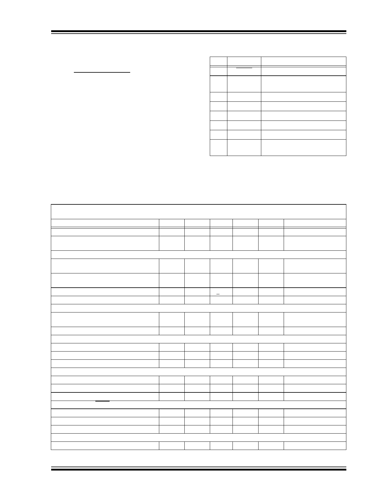
PIN FUNCTION TABLE
Pin
Name
Description
1
SHDN Logic Shutdown
2
GND Battery Management
0V Reference
3
MODE Charge Status Output
4
IMON Charge Current Monitor
5
VBAT Cell Voltage Monitor Input
6
VDRV Drive Output
7
VSNS Charge Current Sense Input
8
VIN
Battery Management
Input Supply
DC CHARACTERISTICS: MCP73827-4.1, MCP73827-4.2
Unless otherwise specified, all limits apply for VIN = [VREG(typ)+1V], RSENSE = 500 mΩ, TA = -20°C to +85°C.
Typical values are at +25°C. Refer to Figure 1-1 for test circuit.
Parameter
Sym
Min
Typ
Max
Units
Conditions
Supply Voltage
Supply Current
VIN
4.5
—
5.5
V
IIN
—
0.5
15
µA Shutdown, VSHDN = 0V
—
250
560
Constant Voltage Mode
Voltage Regulation (Constant Voltage Mode)
Regulated Output Voltage
VREG
4.059
4.1
4.141
4.158
4.2
4.242
V
MCP73827-4.1 only
V
MCP73827-4.2 only
Line Regulation
Load Regulation
Output Reverse Leakage Current
External MOSFET Gate Drive
ΔVBAT
-10
—
10
ΔVBAT
-1
+0.1
1
ILK
—
8
—
mV VIN = 4.5V to 5.5V,
IOUT = 75 mA
mV IOUT=10 mA to 75 mA
µA
VIN=Floating, VBAT=VREG
Gate Drive Current
IDRV
—
—
1
mA Sink, CV Mode
0.08
—
—
mA Source, CV Mode
Gate Drive Minimum Voltage
VDRV
—
1.6
—
V
Current Regulation (Controlled Current Mode)
Current Sense Gain
Current Limit Threshold
Foldback Current Scale Factor
ACS
—
100
—
dB
Δ(VSNS-VDRV) / ΔVBAT
VCS
40
53
75
mV (VIN-VSNS) at IOUT
K
—
0.43
—
A/A
Charge Status Indicator - MODE
Threshold Voltage
Low Output Voltage
Leakage Current
Shutdown Input - SHDN
VTH
—
VREG
—
V
VOL
—
—
400
mV ISINK = 10 mA
ILK
—
—
1
µA
ISINK=0 mA, VMODE=5.5V
Input High Voltage Level
Input Low Voltage Level
Input Leakage Current
Charge Current Monitor - IMON
Charge Current Monitor Gain
VIH
40
—
—
%VIN
VIL
—
—
25
%VIN
ILK
—
—
1
µA
VSHDN=0V to 5.5V
AIMON
—
26
—
V/V ΔVIMON / Δ(VIN-VSNS)
© 2007 Microchip Technology Inc.
DS21704B-page 3
Share Link: