MF0064M-07AT データシートの表示(PDF) - Mitsumi
部品番号
コンポーネント説明
メーカー
MF0064M-07AT Datasheet PDF : 32 Pages
| |||
MITSUBISHI STORAGE CARD
Preliminary
ATA PC CARDS
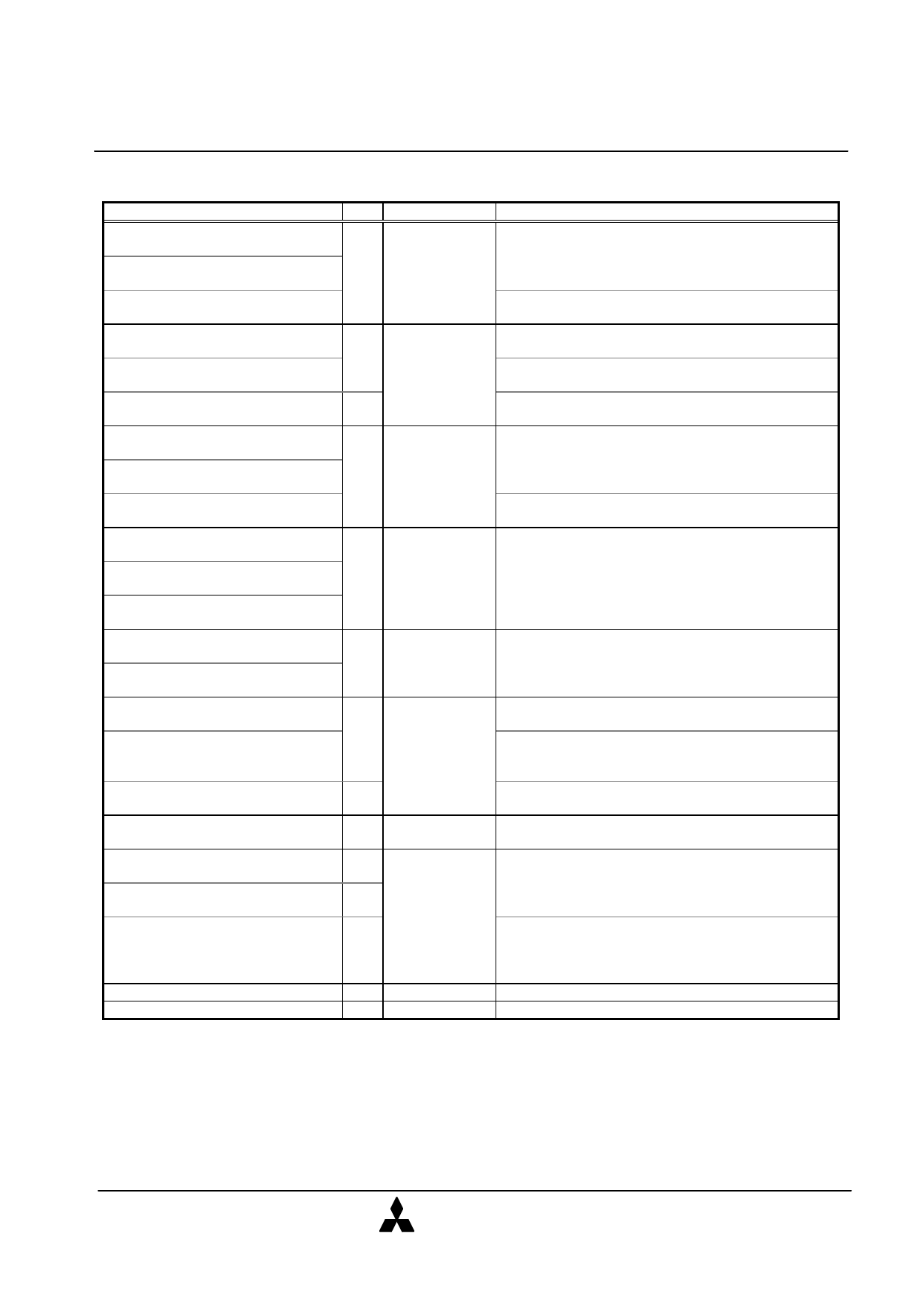
Signal Description(Continued)
Signal Name
I/O
Attribute Memory Select[REG#]
I
(PC Card Memory Mode)
Attribute Memory Select[REG#]
(PC Card I/O Mode)
Attribute Memory Select[REG#]
(IDE ATA Interface)
Battery Voltage Detect[BVD2]
O
(PC Card Memory Mode)
Audio Digital Waveform[SPKR#]
(PC Card I/O Mode)
DASP#
I/O
(IDE ATA Interface)
Card Reset[RESET]
I
(PC Card Memory Mode)
Card Reset[RESET]
(PC Card I/O Mode)
Card Reset[RESET#]
(IDE ATA Interface)
Wait[WAIT#]
O
(PC card Memory Mode)
Wait[WAIT#]
(PC card I/O Mode)
IORDY
(IDE ATA Interface)
Input Port Acknowledge[INPACK#] O
(PC Card I/O Mode)
Input Port Acknowledge[INPACK#]
(IDE ATA Interface)
Battery Voltage Detect[BVD1]
O
(PC Card Memory Mode)
STSCHG#
(PC Card I/O Mode)
Pin No.
61
62
58
59
60
63
PDIAG#
(IDE ATA Interface)
Voltage Sense[VS1, VS2]
I/O
O 43, 57
Cable Select[CSEL]
(PC card Memory Mode)
Cable Select[CSEL]
(PC card I/O Mode)
Cable Select[CSEL]
(IDE ATA Interface)
- 56
-
I
Vcc
GND
- 17, 51
- 1, 34, 35, 68
Description
When this signal is asserted, access is limited to
Attribute Memory with OE#/WE# and I/O Space with
IORD#/IOWR#.
This input signal is not used for this mode and should
be connected to Vcc by the host.
This output is driven to a high-level.
SPKR# is kept negated because this Card does not
have digital audio output.
This signal is the DISK Active/Slave Present signal in
the Master/Slave handshake protocol.
By assertion of this signal, all registers of this Card
are cleared. This signal should be kept to High-Z by
the host for at least 1ms after Vcc applied.
This input pin is the active low hardware reset from
the host.
This signal is asserted to delay completion of the
memory or I/O access cycle.
This signal is asserted when the Card is selected and
can respond to an I/O Read cycle at the
address on the address bus.
This output is driven to a high-level.
This signal is asserted low to alert the host to
changes in the status of Configuration Status
Register in the Attribute Memory Space.
This signal is the Pass Diagnostic signal in the
Master/Slave handshake protocol.
VS1 is grounded so that the Card CIS can be read at
3.3V and VS2 is N.C.
This signal is not used for this mode.
This signal is used to configure this Card as a Master
or a Slave. When this signal is grounded, this Card is
configured as a Master. When this signal is Open,
this Card is configure as a Slave.
5V or 3.3V power.
Ground.
MITSUBISHI
ELECTRIC
4
Oct.1999 Rev. 0.2
Share Link: 