MICRF005 データシートの表示(PDF) - Micrel
部品番号
コンポーネント説明
メーカー
MICRF005 Datasheet PDF : 11 Pages
| |||
MICRF005
Functional Diagram
Micrel
T/R
CAGC
CAGC
ANT
VDD
VSS
RF
Amp
fRX
fIF IF
Amp
fLO
Programmable
Synthesizer
5th Order
Band-Pass Filter
IF
Amp
AGC
Control
Peak
Detector
2nd Order
Low-Pass Filter
Switched-
Capacitor
Resistor
RSC
Compa-
rator
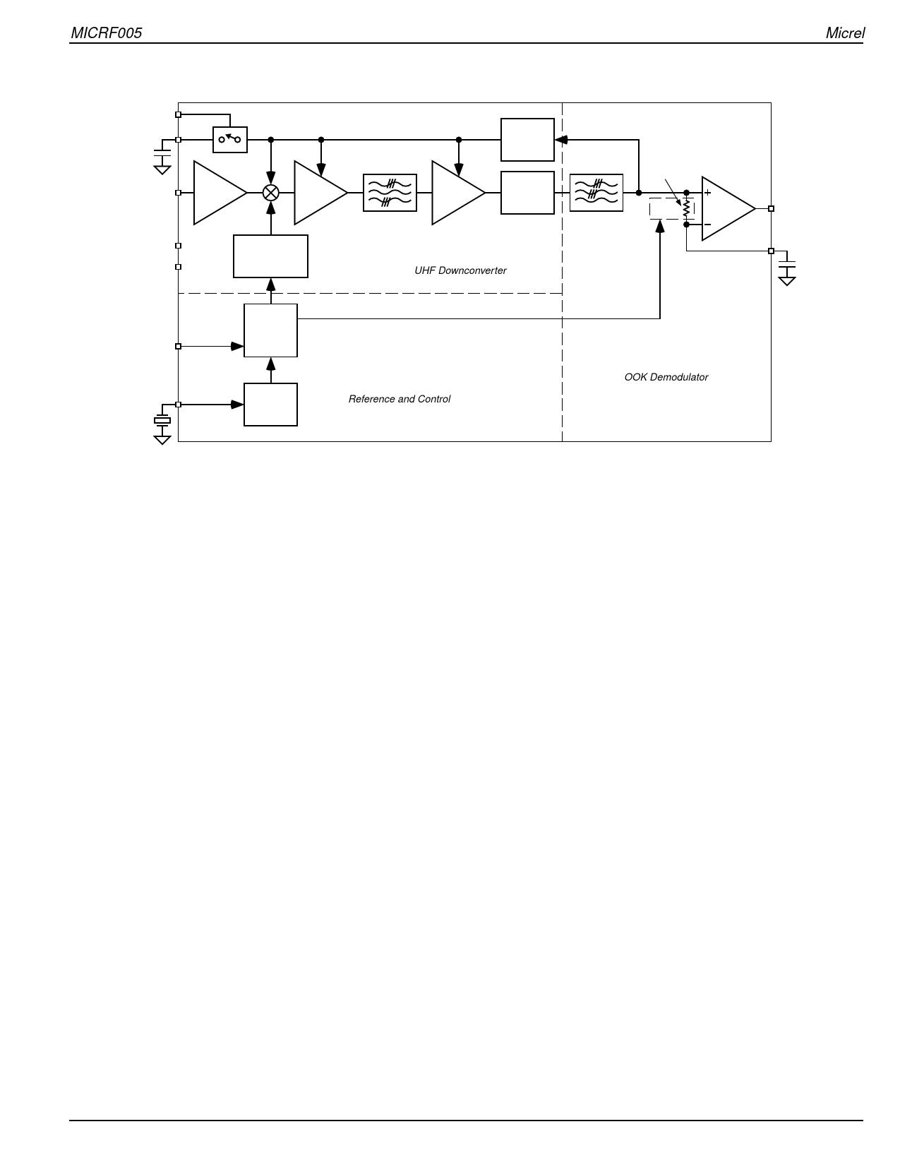
UHF Downconverter
DO
CTH
CTH
SHUT
Control
Logic
REFOSC fT
Crystal
MICRF005
Reference
Oscillator
Reference and Control
MICRF005 Block Diagram
OOK Demodulator
Functional Description
Refer to “MICRF005 Block Diagram”. Identified in the block
diagram are the three sections of the IC: UHF Downconverter,
OOK Demodulator and Reference and Control. Also shown
in the figure are two capacitors (CTH, CAGC) and one timing
component (CR), usually a crystal. With the exception of a
supply decoupling capacitor, these are the only external
components needed by the MICRF005 to construct a com-
plete UHF receiver. Two control inputs are shown in the block
diagram: T/R and SHUT. Through these logic inputs, the user
can control the operation of the IC. These inputs are CMOS
compatible, and are pulled-up on the IC.
IF Bandpass Filter
Rolloff response of the IF Filter is 7th order, while the
demodulator data filter exhibits a 2nd order response.
Slicing Level
Extraction of the dc value of the demodulated signal for
purposes of logic-level data slicing is accomplished using the
external threshold capacitor CTH and the on-chip switched-
capacitor “resistor” RSC, shown in the block diagram. The
effective resistance of RSC is 30kΩ.
Slicing level time constant values vary somewhat with de-
coder type, data pattern, and data rate, but typical values
range from 5ms to 50ms. Optimization of the value of CTH is
required to maximize range.
Squelch
During quiet periods (no signal) the data output (DO pin)
transitions randomly with noise, presenting problems for
some decoders. A simple solution is to introduce a small
offset, or squelch voltage, on the CTH pin so that noise does
not trigger the internal comparator. Usually 20mV to 30mV is
sufficient, and may be introduced by connecting a several-
MΩ resistor from the CTH pin to either VSS or VDD, depending
on the desired offset polarity. Since the MICRF005 has
receiver AGC, noise at the internal comparator input is
always the same, set by the AGC. The squelch offset require-
ment does not change as the local noise strength changes
from installation to installation. Introducing squelch will re-
duce range modestly. Only introduce an amount of offset
sufficient to quiet the output.
Automatic Gain Control
The signal path has AGC (automatic gain control) to increase
input dynamic range. An external capacitor, CAGC, must be
connected to the CAGC pin of the device. The ratio of decay-
to-attack time-constant is fixed at 10:1 (that is, the attack time
constant is 1/10th of the decay time constant). However, the
attack time constant is set externally by choosing a value for
CAGC.
By adding resistance from the CAGC pin to VDDBB or VSSBB
in parallel with the AGC capacitor, the ratio of decay-to-attack
time constant may be varied, although the value of such
adjustments must be studied on a per-application basis.
Generally the design value of 10:1 is adequate for the vast
majority of applications.
To maximize system range, it is important to keep the AGC
control voltage ripple low, preferably under 10mVpp once the
control voltage has attained its quiescent value. For this
reason capacitor values of at least 0.47µF are recommended.
The AGC control voltage is carefully managed on-chip to
allow duty-cycle operation of the MICRF005 in excess of
10:1. When the device is placed into shutdown mode (SHUT
pin pulled high), the AGC capacitor floats, to retain the
voltage. When operation is resumed, only the voltage droop
on the capacitor due to leakage must be replenished, there-
fore a relatively low-leakage capacitor is recommended for
October 2001
5
MICRF005
Share Link: 