MK2722-01S データシートの表示(PDF) - Integrated Circuit Systems
部品番号
コンポーネント説明
メーカー
MK2722-01S Datasheet PDF : 4 Pages
| |||
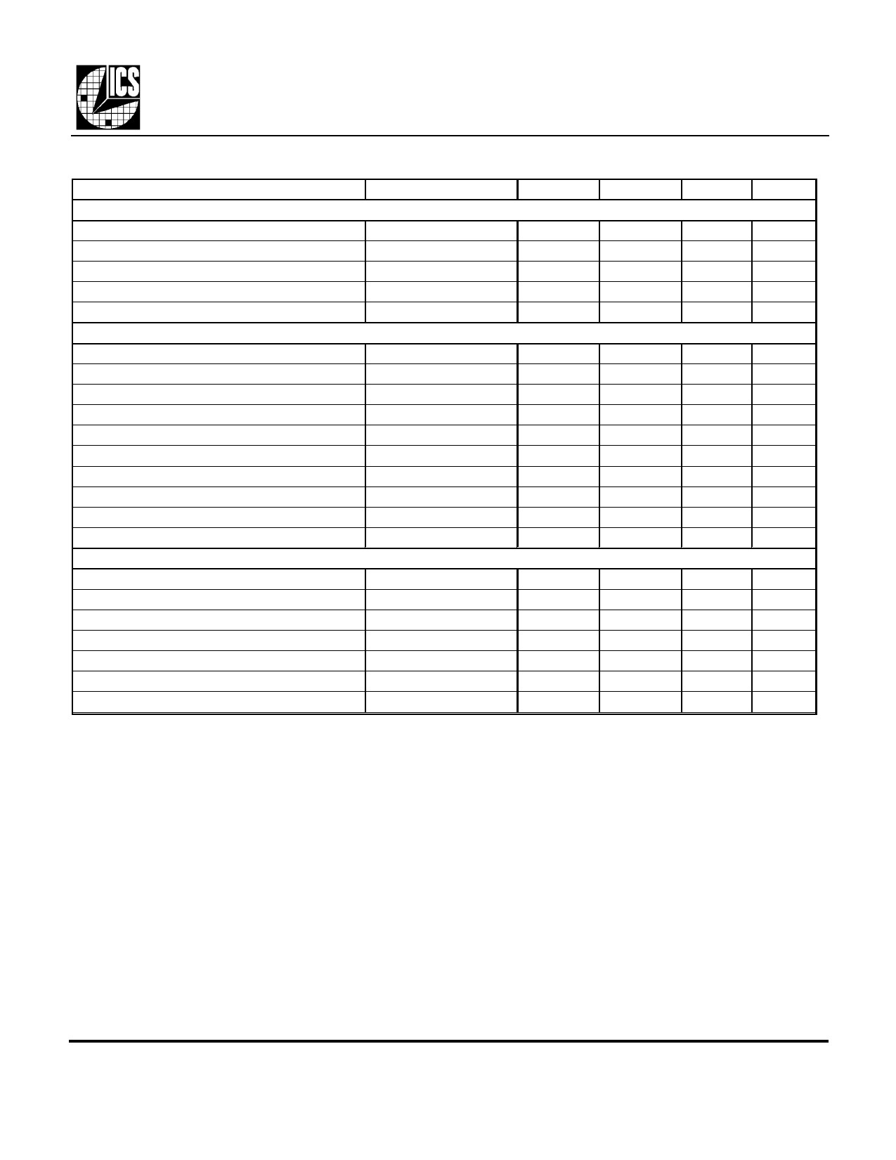
MK2722
Sigma Designs Clock Source
Electrical Specifications
Parameter
Conditions
ABSOLUTE MAXIMUM RATINGS (Note 1)
Supply voltage, VDD
Referenced to GND
Inputs and Clock Outputs
Referenced to GND
Ambient Operating Temperature
Soldering Temperature
Max of 10 seconds
Storage temperature
DC CHARACTERISTICS (VDD = 5V unless noted)
Operating Voltage, VDD
Input High Voltage, VIH
Input Low Voltage, VIL
Output High Voltage, VOH
IOH=-4mA
Output Low Voltage, VOL
IOL=25mA
Operating Supply Current, IDD, 5.0V
No Load
Power Down Supply Current, IDDPD, 5V No Load, note 2
Short Circuit Current
Each output
Input Capacitance
On chip pull-up resistor
Pins 6, 8, 12, 15, and 16
AC CHARACTERISTICS (VDD = 5V unless noted)
Input Frequency
Input Crystal Accuracy
Frequency Error, all clocks
Output Clock Rise Time
0.8 to 2.0V
Output Clock Fall Time
2.0 to 0.8V
Output Clock Duty Cycle
At 1.4V
Maximum Absolute Jitter, short term
Minimum
-0.5
0
-65
4.5
2
VDD-0.4
40
Typical Maximum Units
7
V
VDD+0.5 V
70
°C
260
°C
150
°C
5
5.5
V
V
0.8
V
V
0.4
V
30
mA
25
µA
±50
mA
7
pF
250
kΩ
27.000
MHz
±30
ppm
0
ppm
1.5
ns
1.5
ns
50
60
%
200
ps
Notes: 1. Stresses beyond those listed under Absolute Maximum Ratings could cause permanent damage to the
device. Prolonged exposure to levels above the operating limits but below the Absolute Maximums may
affect device reliability.
2. With AS1=AS0=BS1=BS0=VDD
External Components
The MK2722 requires a minimum number of external components for proper operation. Decoupling capacitors of
0.1µF should be connected between VDD and GND (pins 4 and 5, 13 and 11), as close to the MK2722 as possible.
A series termination resistor of 33Ω may be used for each clock output. If a clock input is not used, a 27 MHz
fundamental mode crystal must be connected as close to the chip as possible. Crystal capacitors should be
connected from pins X1 to ground and X2 to ground. The value (in pF) of these crystal capacitors should be = (CL-
12)*2, where CL is the crystal load capacitance in pF. So for a crystal with 16pF load capacitance, the crystal
capacitors should be 8pF each.
MDS 2722 B
3
Revision 020802
Integrated Circuit Systems, Inc. • 525 Race Street • San Jose • CA • 95126 • (408)295 9800tel • www.icst.com
Share Link: 