ML9041A データシートの表示(PDF) - Oki Electric Industry
部品番号
コンポーネント説明
メーカー
ML9041A Datasheet PDF : 64 Pages
| |||
OKI Semiconductor
PEDL9041A-02
ML9041A-xxA/xxB
Note 3:
Note 4:
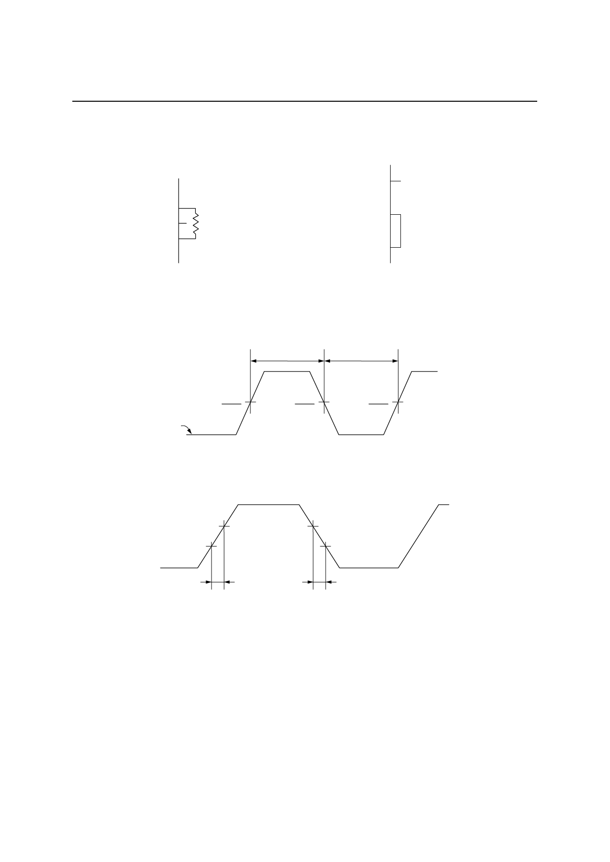
OSC1
OSCR
OSC2
Rf = 180 kΩ±2%
OSC1
OSCR
OSC2
The wire between OSC1 and Rf and the wire between
OSC2 and Rf should be as short as possible.
Keep OSCR open.
The wire between OSC2 and OSCR should be as short
as possible. Keep OSC1 open.
Note 5:
tHW
tLW
Note 6:
fIN
waveform
VDD
VDD
VDD
2
2
2
Applied to the pulses entering from the OSC1 pin
fduty = tHW/(tHW + tLW) ×100 (%)
0.8VDD
0.2VDD
0.8VDD
0.2VDD
trf
tff
Applied to the pulses entering from the OSC1 pin
Note 7:
The maximum value of the voltage multiplier input voltage should be set at 3.5 V, and the
minimum value of the voltage multiplier input voltage should be set so that the voltage
multiplier output voltage meets the specification for the bias voltage for driving LCD after
contrast adjustment.
Note 8: If using the built-in contrast control circuit, control the circuit so that the voltage of VDD-V5 is the
minimum value of the bias voltage for driving LCD or higher.
Note 9: For 1/4 bias, V2 and V3B pins are short-circuited. V3A pin is open.
For 1/5 bias, V3A and V3B pins are short-circuited. V2 pin is open.
10/64
Share Link: 